On the production line of the SMT assembly plant, reflow soldering is a difficult process in the BGA assembly process. Setting process parameters and obtaining a suitable temperature profile are very important for good BGA soldering. Due to the different packaging forms of BGA, the thermal resistance of CBGA is larger than that of PBGA, so to reach the same temperature, CBGA requires a higher temperature setting and longer preheating time than PBGA. For tin-lead solder paste and lead-free solder paste, the temperature setting and heating time are significantly different.
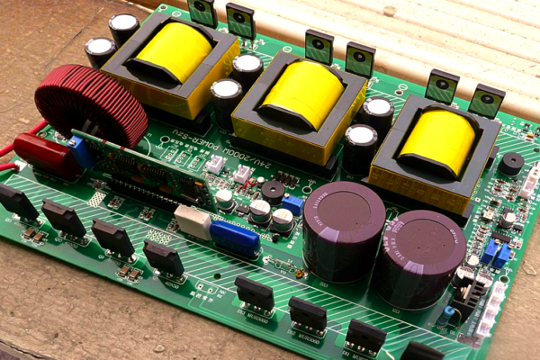
reflow soldering machine
Table of Contents
1. Pre-heating stage
The main purpose of preheating is to heat the PCB and its components uniformly, and at the same time have a baking effect on the PCB and components, remove the moisture in it, and evaporate the appropriate amount of flux in the solder paste. The heating rate in the preheating stage cannot be too fast to prevent the PCB from being heated too fast and causing greater deformation. Generally, the heating rate is controlled at 3℃/s, and the preheating time is between 60-90s.

2. Activation stage
The main purpose of this stage is to activate the flux in the solder paste, remove the oxides on the surface of the pad and the surface of the solder paste alloy, to achieve a clean metal surface and prepare for the solder paste reflow process. At the same time, the excessive flux in the solder paste is evaporated and the PCB is preheated to prevent the PCB from deforming due to excessive heating during the reflow process. For tin-lead soldering, the temperature at this stage should be kept at 60-120S at 150-180℃; for lead-free soldering, the temperature at this stage should be kept at 60-180S at 160-200℃, so that the flux can fully play its role. The temperature rise rate in the activation stage is generally controlled at 0.3 plus. 5°C/s.
3. Reflow stage
At this stage, the temperature of the solder joint has risen above the melting point of the solder paste, and the solder paste is in a molten state. The main purpose of the reflow stage is to wet the solder pads and the pins of the components to achieve good soldering requirements. For PBGA, the solder balls are Sn63Pb37, Sn62Pb36Ag2, and Sn96.5Ag3.0Cu0.5 alloys. During the reflow process, the solder balls and solder paste are melted and mixed to form solder joints; for CBGA, the solder balls are Snl0Pb90 high-temperature alloys. The solder ball does not melt during the reflow process, the solder paste melts and wets the pad and the high-temperature solder ball to form a solder joint. Therefore, it takes a suitable time to ensure that the molten solder paste can well wet the pads and solder balls. Too short a time may cause poor wetting to form a pseudo solder, and too long may cause a thick formation between the solder and the pad, a layer of intermetallic compounds Cu6sn5 and Cu3Sn, due to its brittleness, is easy to form cracks and cause solder joint failure. Especially for lead-free electronic assembly, due to the high content of element Sn in lead-free solder alloying, it is easier to form thicker intermetallic compounds at high temperature and cause the failure of solder joints. For SnPb soldering, the time above the melting point of 183℃ is generally controlled in 60-90s, where the peak temperature is within the range of 210-225°C and the time is controlled within 10-20s; for lead-free soldering, it is generally required to control the time above the melting point of 217-219°C within 60-120s, and the peak temperature 230-235℃ is better to control the time in the range of 20-40s.
reflow temperature profile
4. Cooling stage
After the solder paste is reflowed, the flux is completely consumed, forming a molten metal solder joint. The main purpose of the cooling stage is to refine the crystal grains while the solder joints are solidified, inhibit the growth of intermetallic compounds, and improve the strength of the solder joints. However, too fast cooling rate will cause PCB deformation and thermal cracking of electronic components, especially for components with large heat absorption such as BGA, too fast cooling rate will easily cause damage to the internal package, leading to BGA failure. Generally, the cooling rate is controlled within 1-3℃/s.
Get your exclusive quote immediately: fill out the form or send an email directly.As a professional PCB manufacturer for hobbyist , we will provide you with a quote service within 24 hours. Enjoy free DFM optimization and a 10% discount on SMT patches for your first order!