Import Netlist
The process of transferring a netlist from schematic layout software to PCB design CAD software.
Inner Layer
Layers within a circuit board that are situated between the outer copper layers. These layers can be trace layers or ground plane layers.
Lead
The part surrounding the component hole or through-hole.
Lead-Free Solder
These solders are based on 95% tin metal with small additions (about 1%) of silver, copper, bismuth, and other metals. The standard tin/lead solder is 60% tin, 40% lead. Most lead-free solders have a melting point about 30/35 degrees Celsius higher than 60/40 tin/lead solder. Thus, the soldering process must be conducted at around 255 degrees Celsius instead of a more normal 235 degrees Celsius. Most components have a maximum temperature rating of 260 degrees Celsius, limiting the use of optimal temperatures.
Legend
The silkscreen component identification layer, sometimes referred to as “identification.”
Microsection
A polished sample of a PCB cross-section, typically through a PTH hole, usually mounted in a transparent resin. Under a magnifying lens, microsections are used to verify the integrity of plating along the hole.
Mil
One thousandth of an inch.
Mixed Technology
An assembly process used when through-hole pin, surface mount, and other mounting technologies are placed on the same printed circuit board.
MLPCB
See Multilayer Printed Circuit Board.
Moisture Absorption
Moisture is the enemy of printed circuit boards. Absorbed moisture raises the Dk value, causes board swelling, and leads to thermal defects like substrate blistering and pad cracking during soldering. If storage time is short, or humidity is low, moisture is not an issue. However, if PCBs are stored in a high humidity environment for months or longer, they should be separated, stored, and baked at 120 degrees Celsius for 1 hour before assembly.
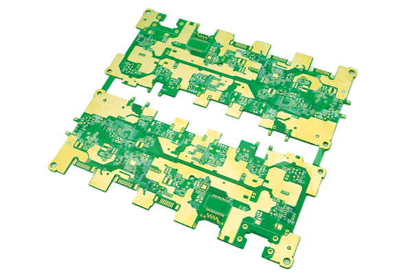
Multilayer Board
A PCB with more than 2 layers.
Multilayer Printed Circuit Board
A printed circuit board with more than 2 layers, typically 4-layer, 6-layer, or 8-layer. The internal layers can be ground plane layers, trace layers, or a mixture of both. Interlayer connections are achieved through copper-plated through-holes.
Major Defect
A defect that is likely to cause failure of the unit or product.
Master Drawing
A document showing all part dimension limitations or grid positions on a PCB. The conductor and non-conductive materials of the PCB (such as dielectrics, solder mask, etc.) are also shown.
Delamination
An internal condition of the laminate base material where the glass fiber separates from the resin at weave intersections. This condition manifests as discrete white spots under the base material surface. It is often caused by thermal stress.
MELF, Metal Electrode Leadless Face
A cylindrical component package with metallized terminals at each end for surface mounting. This package is typically used for diodes, capacitors, and resistors.
Metallization
Depositing metal, either on its own or over a base metal, to achieve electrical and mechanical interconnections.
Mixed Mount Technology
An assembly mounting technology that simultaneously uses both through-hole and surface mount components, placed on the same package and interconnection structure.
Multilayer Board
A printed wiring board using more than two layers for routing traces. Inner layers are connected to outer layers through copper-plated through-holes.
Net
All points connected together by copper.
Net Endpoint
A pad or plated through-hole at the end of a branch of a circuit.
Netlist
A list of net numbers and their associated X and Y coordinates, along with the surfaces they are located on. This is the basic information for building a test program for an electrical test machine, as it physically determines the locations of the nets to be tested. Another type of netlist is the CAD software design package netlist, which identifies the connections between components but not their physical locations.
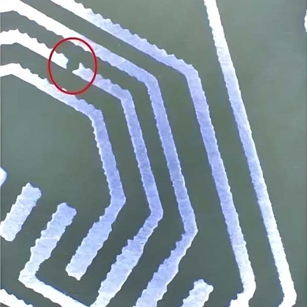
Nick
A cut or notch on a trace or pad.
Neutralizer
An alkaline chemical added to water to improve its ability to dissolve organic acid flux residues.
Non-Wetting
A condition where a surface has been in contact with molten solder but the solder has not completely “wet” the surface. The base metal remains exposed. Non-wetting is primarily due to impurities acting as physical barriers (intermetallic compounds or oxides) preventing surface bonding.
Open Circuit
An absence of expected circuit continuity. Two electrically connected points become electrically separated during manufacturing, often due to over-etching or misalignment.
Organic Coating
Organic Solderability Preservatives (OSP) are organic compounds that selectively bond to copper to form a protective layer over the copper. Benzimidazole, benzotriazole, imidazole, or substituted benzimidazole are commonly used to limit copper oxidation. Organic materials react with copper to form a thin coating that prevents moisture and air from contacting the copper surface, preserving solderability. OSPs are inexpensive but not mechanically robust and cannot withstand multiple heat cycles.
Outgassing
De-aeration or other gaseous emissions from a PCB or solder joint during heating.
Pricing
Pricing varies by factory due to differences in materials, processes, and labor costs. For example, using high-quality base material like KB “A-level” and superior chemicals in plating processes like ROHM HRRS increases costs but ensures reliability. Long-term competitiveness is maintained through stable, professional staff with higher salaries and training.
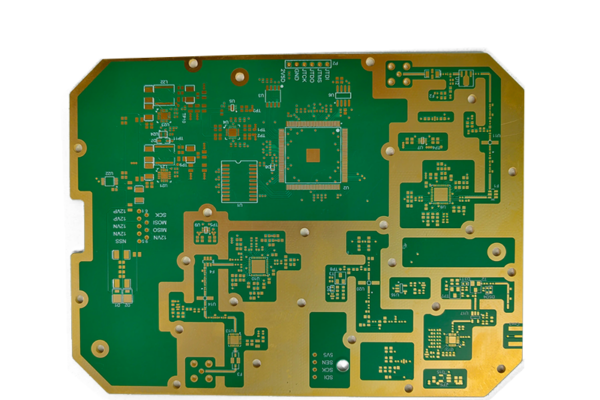
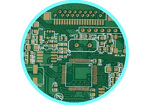
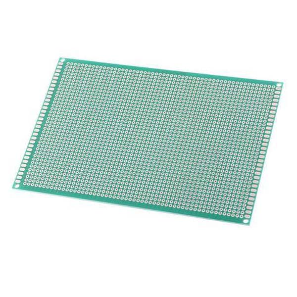
Printed Circuit Board (PCB)
A sheet of glass-reinforced plastic with etched copper patterns providing electrical interconnections between electronic components, which are soldered to copper pads or mounted through holes in the PCB.
Pad
The portion of the conductive pattern on PCBs designated for mounting or attaching components.
Panel
A piece of laminate containing multiple PCB images.
PCB Prototype
An initial low-volume production run of PCBs.
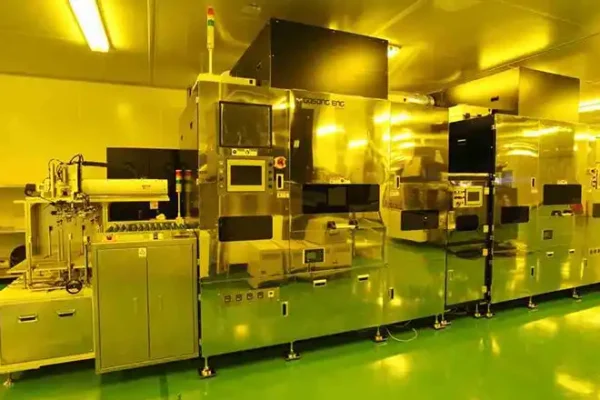
Photomechanical Department
The department in a PCB factory that uses photosensitive materials to print images on PCBs.
Photoplotter
A machine for creating photographic images of PCBs from electronic data.
Photoresist or Plating Resist
A light-sensitive film that hardens when exposed to UV light under a photographic mask. Unexposed areas are washed away with alkaline chemicals, often in a conveyorized processor.
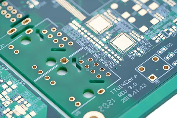
Plated Through Hole (PTH)
A hole in which electrical connection is made between internal or external conductive patterns, or both, by metal plating on the hole wall.
Polyimide Laminate
A high-temperature laminate system with a Tg around 250 degrees Celsius, suitable for applications with operating temperatures over 200 degrees Celsius.
PWB (Printed Wiring Board)
Another term for PCB, emphasizing the wiring aspect of the board.
Resist
A coating material used to mask or protect selected areas of a PCB from etching or plating processes.
Router
A machine that profiles laminate to the shape and size of the required PCB.
RS-274-X
A variant of Gerber data that includes aperture shape information along with the usual tool selection and movement commands.
Set-Up Charge (NRE Charge)
A one-time fee for engineering and artwork film setup unless the Gerber file changes. Engineers check the Gerber file for errors against production capabilities and translate it into tools and language for production. The lines and solder mask are produced similarly to a camera needing film, unique for each PCB.
Scoring
Partially cutting through laminate with twin rotary cutters, leaving a thin material web that can be broken by snapping after assembly.
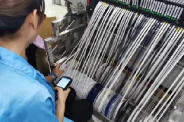
Screen Printing
Transferring a pattern onto a surface by forcing suitable material through a screen with a squeegee.
Short Circuit
Erroneous low-resistance connections between two or more nets or isolated points.
Silver Finish
A silver coating used instead of HASL, consisting of a submicron silver deposit with an organic top layer to prevent tarnishing and maintain solderability. It combines metallic and organic coating benefits without drawbacks, providing good solderability, flat and uniform topography, and a bright appearance. During soldering, the silver dissolves into the joint, forming a bond directly with the copper surface.
Single-Sided Board
A PCB with components on only one side.
SMOBC (Solder Mask Over Bare Copper)
A modern process distinguishing it from “solder mask over tin/lead.”
SMT (Surface Mount Technology)
A technology where components are mounted directly onto PCBs without wires passing through holes. Most modern PCBs use SMD technology.
Teardrop
A pad shape that tapers evenly into its associated trace.
Tester
A machine that checks a PCB’s circuit connectivity against the design netlist.
Thermal Relief
Connecting through-holes to ground planes via thermal relief pads to prevent the ground plane’s heat sink effect from interfering with sufficient soldering temperatures.
Trace
An electrical connection between two or more points on a PCB.
Underwriters Laboratories (UL)
A U.S.-based safety standard certification organization. U.S. insurance companies require UL approval for product liability insurance. For electrical goods, UL focuses on fire hazards and electrical insulation. FR4 laminate is approved to the 94-V0 rating.
Via Holes
Via holes are plated through holes in a printed circuit board (PCB) that create electrical connections between different layers of the PCB. These holes do not have component leads inserted into them.
Blind Via Holes
Blind via holes are a type of plated through hole that connects an outer layer of a PCB to one or more inner layers without passing through the entire board. Like via holes, these do not have component leads inserted into them.