In today’s highly integrated electronic devices, the quality of PCB design directly affects product performance and reliability. This article systematically outlines the six core principles of PCB design, covering key aspects such as layout optimization, signal integrity assurance, and manufacturing processes, providing engineers with practical design guidance.
Table of Contents
1、 Layout Design: Functional Zoning and Space Optimization
1. Dimensional planning and mechanical strength
The PCB size should balance heat dissipation and anti-interference ability, with a recommended aspect ratio of 3:2 or 4:3. When it exceeds 200 × 150mm, mechanical strength should be considered, and the distance between edge components and the board edge should be ≥ 2mm to prevent damage to the board.

2. Layout of high-frequency and sensitive components
High frequency components (such as crystal oscillators) need to shorten the wiring and control the spacing within 1/20 of the wavelength to reduce distributed parameter interference. The input/output ports should be kept away, and sensitive components (such as ADCs) should be kept at a distance of ≥ 5mm from noise sources (such as switching power supplies).
3. Thermal management strategy
Heating elements (such as power MOSFETs) are prioritized to be arranged at the edge of the board, with a heat dissipation via matrix (≥ 10/cm ²) added below and connected to the inner copper plane. The temperature rise can be reduced by 15 ℃. Thermistors should be kept away from heat sources, and external heat sinks are recommended for high-power devices.
2、 Wiring Design: Signal Integrity and EMC Optimization
1. Line width and current carrying capacity
The width of the power line and ground line is ≥ 1.5mm (2A current), and the high-frequency signal line width is calculated according to the impedance formula (such as about 0.3mm for a 50 Ω microstrip line under FR-4 substrate). The line width of digital circuits can be reduced to 0.02-0.3mm, but sudden changes in line width should be avoided.
2. Corner and Intersection Processing
The wire corners are designed with a 135 ° arc to avoid impedance jumps caused by right angles. The cross line is solved by “drilling and winding” or adding isolated ground wires, and the high-speed differential signal is strictly equal in length (with an error of ± 0.05mm).
3. Application of 3W/20H principle
The key signals (such as clock lines) follow the 3W spacing rule (line spacing ≥ 3 times line width), and the power layer is compressed by 20H relative to the ground layer (H is the thickness of the medium), effectively suppressing edge radiation.
3、 Power and ground wire design: key to noise suppression
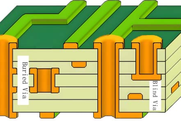
1. Hierarchical architecture and decoupling capacitors
The multi-layer board adopts a “signal ground power signal” stack, with the power layer adjacent to the formation to reduce impedance. 0.1 μ F ceramic capacitors (spacing ≤ 2mm) are arranged next to the IC power pins, and 10 μ F energy storage capacitors are configured for every 10 chips.
2. Grounding strategy
The digital ground is connected to the analog ground at a single point, and the high-frequency circuit is grounded with large-area copper cladding. Ground wire width ≥ 3mm, minimize loop area, and install grounding via “fences” on both sides of sensitive signals.
3. Power integrity
The high current path (such as motor drive) uses 2-4oz thick copper, and the via adopts a “honeycomb” layout to reduce impedance. The multi power system is isolated by magnetic beads or LC filters to avoid plane overlap.
4、 EMC and Signal Integrity Assurance
1. Shielding and grounding design
High speed signals (such as USB 3.0) adopt a strip line structure with ground planes on both sides. Sensitive circuits are treated with ‘ground wrapping’, and critical signals are kept at least 6.4mm away from the I/O interface.

2. Loop control
The signal line and its return path form the minimum loop, with differential pairs running in parallel and matching in length. Avoid signals crossing the ground plane segmentation area and add splicing capacitors (10-100nF) if necessary.
3. Interference suppression
Adjacent layers are arranged orthogonally, with parallel routing length ≤ 3cm. When using serpentine routing, the spacing should be ≥ 4 times the line width, and inserting ground wires to isolate and reduce coupling.
5、 Manufacturing process and reliability verification
1. DFM compatibility
Line width/spacing ≥ 6mil, through-hole inner diameter ≥ 8mil, solder pad outer diameter ≥ aperture+1.2mm. Avoid sharp angle wiring, and use grid shaped copper foil to prevent thermal expansion.
2. Welding and Testing
The distance between SMT component pads and vias is ≥ 25mil, and the peak temperature of reflow soldering is adjusted according to the packaging (such as SOT-23 ≤ 245 ℃). X-ray inspection shows that the porosity of solder joints is less than 15%, and functional testing covers signal integrity (such as eye diagram testing) and environmental reliability (-40 ℃~125 ℃ cycling).
3. Material selection
Low loss substrates such as Rogers RO4350B (Dk=3.48) are preferred for high-frequency scenarios, and high TG materials (Tg ≥ 170 ℃) are used for automotive electronics and certified by AEC-Q200.
By following the above principles, the reliability, efficiency, and anti-interference ability of PCB design can be significantly improved. In cutting-edge fields such as 5G communication and new energy vehicles, PCB design will continue to break through performance boundaries by combining simulation tools (such as HFSS, HyperLynx) with new material technologies.