In high-speed electronic devices and power management systems, the selection of NMOS (N-type MOS transistor) and PMOS (P-type MOS transistor) as core switching elements directly affects circuit efficiency and reliability. This article comprehensively analyzes the differences between structural characteristics, performance parameters, and application scenarios to assist engineers in optimizing PCB design.
Table of Contents
1、 Differences in structure and conduction mechanism
1. Channel type and charge carriers
-NMOS: Based on N-channel, it mainly relies on electronic conductivity. When the gate voltage (Vgs) is higher than the source voltage and exceeds the threshold voltage (Vth), electrons form a conducting channel on the surface of the P-type substrate, and the current direction is from the drain (D) to the source (S).
-PMOS: adopts a P-type channel with holes as carriers. The conduction condition is that the gate voltage is lower than the source voltage (Vgs<Vth), and the current direction is from the source (S) to the drain (D).

2. Requirements for driving voltage
NMOS typically requires a positive voltage drive (such as 5V or 10V), while PMOS requires a negative voltage or a gate voltage lower than the source. This feature makes PMOS easier to implement in high-end drivers (such as power supply positive control), but additional attention needs to be paid to gate voltage matching.
2、 Performance comparison and selection key
1. Conducting resistance and power consumption
-The electron mobility of NMOS is 2-3 times that of holes, and the on resistance (Rds (on)) at the same size is only 1/3 to 1/2 of that of PMOS. For example, the Rds (on) of a certain manufacturer’s NMOS model can be as low as 0.29m Ω, while the lowest for PMOS is 3m Ω, resulting in significant efficiency advantage of NMOS in high current scenarios.
-PMOS is commonly used in low-power or static bias scenarios, such as complementary designs in CMOS circuits, due to its high conduction loss.
2. Switching speed and high-frequency adaptability
-The electronic mobility advantage of NMOS makes its switching speed faster, suitable for high-frequency applications such as DC-DC converters and 5G RF modules, with switching losses reduced by more than 30% compared to PMOS.
-PMOS is suitable for low-frequency or non real time control circuits due to its low hole mobility and long switching delay.
3. Thermal management and reliability
-NMOS is susceptible to thermal excitation at high temperatures and requires optimized heat dissipation design (such as heat dissipation via arrays or thick copper layers); PMOS has better high temperature resistance and is suitable for harsh environments such as automotive electronics.
3、 Typical application scenarios and design strategies
1. Low edge drive and high edge drive
-NMOS: As a low side switch (source grounded), it is widely used in scenarios such as motor driving and LED control. For example, in DC-DC buck circuits, the high-frequency switching capability of NMOS can improve energy efficiency by over 95%.
-PMOS: As a high side switch (with the source connected to the power supply), it simplifies the control logic, but attention should be paid to the leakage problem caused by parasitic diodes. In multi power systems, substrate gating technology can be used to block the leakage path.
2. Complementary applications and cost balance
-CMOS circuit: Combining the complementary characteristics of NMOS and PMOS to achieve low-power digital logic (such as microcontrollers). For example, in an inverter, NMOS is responsible for pull-down and PMOS is responsible for pull-up, resulting in almost zero static power consumption.
-Cost considerations: Due to low wafer utilization, PMOS has a 20% -50% higher cost than NMOS under the same specifications. In power management, the NMOS+charge pump scheme is often used to replace PMOS, balancing performance and economy.
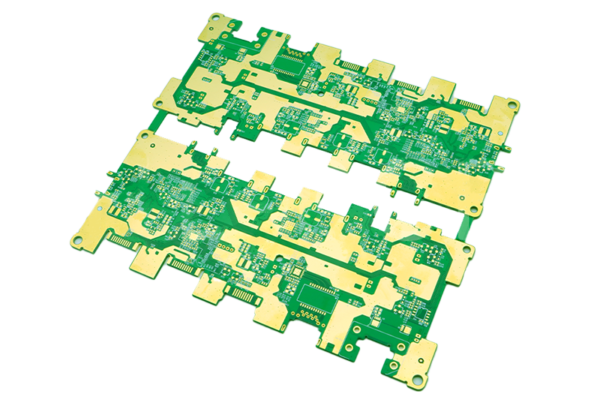
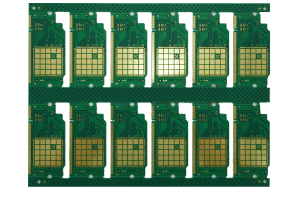
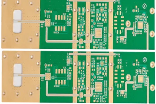
4、 Optimization points in PCB design
1. Layout and EMC protection
-When driving inductive loads with NMOS, it is necessary to use body diodes for freewheeling, and shorten the circuit path during layout to reduce radiation.
-In high-end driving, PMOS requires a grounded design for sensitive signal lines, with grounding vias arranged on both sides to suppress crosstalk.

2. Parasitic parameter control
-In high-frequency scenarios, the gate parasitic capacitance (Cgs, Cgd) of NMOS needs to be quickly charged and discharged through a low impedance driving circuit to avoid switch delay. For example, using a driver IC with an integrated charge pump to enhance transient current.
3. Heat dissipation design
-A heat dissipation via array (≥ 10/cm ²) is arranged below the high-power NMOS, connected to the inner copper plane, and the temperature rise can be reduced by 15 ℃.
5、 Industry Trends and Innovative Technologies
1. Third generation semiconductor materials
SiC and GaN based NMOS devices break through traditional silicon-based limitations, with voltage resistance increased to over 1200V, suitable for electric drive systems in new energy vehicles.
2. Intelligent driver integration
An intelligent MOS module integrating temperature sensing and adaptive gate drive, which can dynamically adjust switch speed, balance efficiency and EMI.
By understanding the core differences between NMOS and PMOS, engineers can accurately select and optimize circuit performance and cost. In fields such as 5G communication and new energy, combining new materials and intelligent control technology, the application of MOS transistors will become more efficient and reliable.