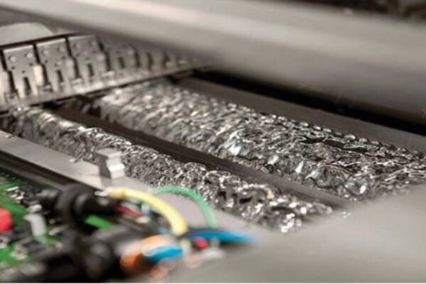
As the “invisible skeleton” of electronic products, printed circuit boards (PCB Manufacturing) run through almost every corner of modern life. From smartphones, laptops to smart home appliances, PCBs connect electronic components through precisely arranged conductive lines, becoming the “nervous system” for device operation.
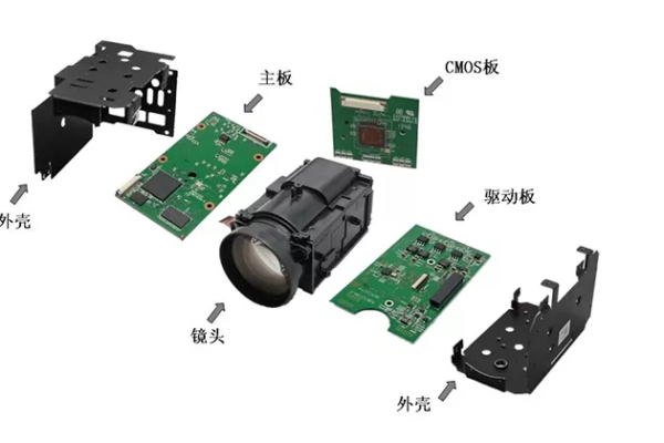
In the field of consumer electronics, PCB Manufacturing support high-frequency communication for mobile phones, data processing for computers, and even flexible design for wearable devices. For example, the curved circuit board of a smartwatch relies on flexible PCBs (FPC) to achieve slimness. In automotive electronics, PCBs are not only used in traditional in car entertainment systems, but also play a key role in battery management systems (BMS) and autonomous driving sensors for new energy vehicles, ensuring high reliability and safety. In addition, precision monitoring of medical equipment, industrial automation control, and even high-frequency signal transmission of aerospace equipment all rely on the technical support of multi-layer PCBs and rigid flexible composite boards.


The prospect of PCB manufacturing
With the popularization of 5G, IoT, and artificial intelligence, the PCB Manufacturing industry is ushering in a new round of transformation. On a technical level, high-density interconnect (HDI) and ultra-thin substrate (SLP) technologies will drive further miniaturization of electronic products, while high-frequency high-speed PCBs will meet the transmission needs of 6G communication and autonomous driving. The application scenarios of flexible PCBs will also expand, such as foldable screens and implantable medical devices, bringing more possibilities for design with their flexibility and durability. Under the trend of environmental protection, the popularization of green processes such as lead-free soldering and biodegradable materials will help the industry achieve sustainable development.
Market expansion and intelligent upgrading
It is predicted that the PCB Manufacturing market size will exceed 800 billion yuan by 2030, with growth driven by emerging fields such as new energy and data centers. The introduction of intelligent manufacturing and automated production lines, such as AI driven quality inspection systems, will improve efficiency and reduce costs. At the same time, the demands of satellite communication, low orbit Internet and other frontier fields will promote the innovation of high-frequency PCB and 3D packaging technology.
In summary, PCB is not only the cornerstone of modern technology, but also continues to evolve through technological iteration and green transformation. In the future, with the deep integration of intelligence and environmental protection concepts, this “invisible skeleton” will support a broader digital world.