Table of Contents
Introduction to Gold Finger PCBs
In the world of electronics and printed circuit boards (PCBs), there’s a crucial component that often goes unnoticed by the average consumer but plays a vital role in the functionality of many devices we use daily. This component is known as the Gold Finger PCB. But what exactly are Gold Finger PCBs, and why are they so important in the electronics industry?
Gold Finger PCBs are specialized printed circuit boards that feature gold-plated connectors along one or more edges. These gold-plated connectors, aptly named “gold fingers,” serve as a critical interface between the PCB and other electronic components or devices. The use of gold in these connectors is not just for show; it serves a very specific and important purpose in ensuring reliable electrical connections and optimal performance of electronic devices.

The Anatomy of Gold Finger PCBs
What Are Gold Fingers?
Gold fingers are narrow, gold-plated strips that run along the edge of a printed circuit board. These fingers are typically arranged in a parallel formation and are designed to make contact with corresponding connectors in a mating device or socket. The gold plating on these fingers is not just a thin layer; it’s a carefully applied coating that adheres to strict specifications to ensure optimal performance.
The Structure of Gold Fingers
The structure of gold fingers is more complex than it might appear at first glance. Each gold finger consists of several layers:
Base Material: This is typically the same material as the rest of the PCB, often FR-4 (a type of fiberglass).
Copper Layer: A layer of copper is applied to the base material, forming the conductive path.
Nickel Layer: A thin layer of nickel is often applied over the copper. This serves as a barrier layer and improves adhesion of the gold plating.
Gold Plating: The final layer is the gold plating itself. This can be applied using various methods, including electroplating or electroless plating.

The Importance of Gold in PCB Connectors
Why Use Gold?
Gold is chosen for these connectors for several crucial reasons:
Corrosion Resistance: Gold is highly resistant to corrosion and oxidation, ensuring that the connectors remain functional over long periods.
Excellent Conductivity: Gold is an excellent conductor of electricity, allowing for efficient signal transmission.
Durability: Gold is a soft metal, but when used in the right thickness, it provides a durable surface that can withstand multiple insertions and removals.
Low Contact Resistance: Gold offers very low contact resistance, which is crucial for maintaining signal integrity, especially in high-frequency applications.
The Gold Plating Process
The process of applying gold to PCB connectors is a precise and controlled procedure. It typically involves the following steps:
Cleaning: The PCB is thoroughly cleaned to remove any contaminants.
Masking: Areas that should not be plated are masked off.
Activation: The surface is activated to ensure proper adhesion of the plating.
Plating: Gold is electroplated onto the exposed copper traces.
Thickness Control: The thickness of the gold layer is carefully controlled, typically ranging from 30 to 50 microinches.
Applications of Gold Finger PCBs
Gold Finger PCBs find applications in a wide range of electronic devices and industries. Some common applications include:
Computing Devices
One of the most prevalent uses of Gold Finger PCBs is in computing devices. They are commonly found in:
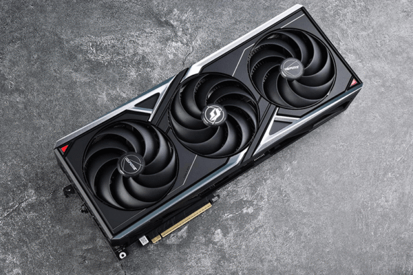
Motherboards: For connecting expansion cards like graphics cards, sound cards, and network adapters.
Memory Modules: RAM sticks use gold fingers to connect to the motherboard.
Hard Drives and SSDs: Many storage devices use gold fingers for their interface connections.
Telecommunications
In the telecommunications industry, Gold Finger PCBs are used in:
Network Switches and Routers: For connecting various network cards and modules.
Cellular Base Stations: In equipment that requires reliable, high-speed connections.
Consumer Electronics
Gold Finger PCBs are also prevalent in many consumer electronic devices:
Smartphones and Tablets: For connecting various internal components and expansion modules.
Gaming Consoles: In memory cards, game cartridges, and internal components.
Digital Cameras: For memory card slots and connecting to computers.
Automotive Electronics
The automotive industry increasingly relies on Gold Finger PCBs for:
Engine Control Units (ECUs): For reliable connections in harsh environments.
Infotainment Systems: In removable navigation and entertainment modules.
Aerospace and Defense
In these high-reliability applications, Gold Finger PCBs are used in:
Avionics Systems: For critical flight control and navigation equipment.
Satellite Communications: In equipment that must function reliably in space.
The Manufacturing Process of Gold Finger PCBs
The production of Gold Finger PCBs involves several specialized steps beyond standard PCB manufacturing:
Design Considerations
When designing a PCB with gold fingers, several factors must be considered:
Finger Width and Spacing: The width of each finger and the space between them must be precisely calculated to ensure proper mating with the connector.
Beveled Edge: The edge of the PCB where the gold fingers are located is often beveled to facilitate smooth insertion into connectors.
Plating Area: The area to be gold-plated must be clearly defined in the PCB design.
PCB Fabrication
The initial stages of fabrication are similar to standard PCBs:
Substrate Preparation: The base material (usually FR-4) is prepared.
Copper Layering: Copper foil is laminated onto the substrate.
Etching: The copper is etched to create the desired circuit pattern.
Gold Plating Process
The gold plating process is what sets Gold Finger PCBs apart:
Nickel Plating: A layer of nickel is first applied to the copper traces where gold fingers will be located.
Gold Plating: Gold is then electroplated over the nickel layer. This is typically done using a hard gold plating process for durability.
Thickness Control: The thickness of the gold layer is carefully controlled, typically ranging from 30 to 50 microinches.
Quality Control
Rigorous quality control measures are implemented:
Visual Inspection: Each board is visually inspected for defects.
Thickness Testing: The thickness of the gold plating is measured to ensure it meets specifications.
Electrical Testing: The conductivity and resistance of the gold fingers are tested.
Advantages of Gold Finger PCBs
Gold Finger PCBs offer several significant advantages:
Reliability
The use of gold ensures a reliable electrical connection even after multiple insertions and removals.
Longevity
Gold’s resistance to corrosion means that Gold Finger PCBs can maintain their performance over extended periods.
Signal Integrity
The excellent conductivity of gold helps maintain signal integrity, which is crucial in high-speed applications.
Versatility
Gold Finger PCBs can be designed for a wide range of applications and environments.
Challenges and Considerations
While Gold Finger PCBs offer many advantages, there are also some challenges to consider:
Cost
The use of gold increases the cost of manufacturing, which can be a significant factor in high-volume production.
Environmental Concerns
The gold plating process can involve chemicals that require careful handling and disposal.
Design Complexity
Designing PCBs with gold fingers requires additional considerations and expertise.
Future Trends in Gold Finger PCB Technology
As technology continues to evolve, so too does the field of Gold Finger PCBs:
Miniaturization
As devices become smaller, there’s a trend towards miniaturizing gold fingers while maintaining their performance.
Alternative Materials
Research is ongoing into alternative materials that could provide similar benefits to gold at a lower cost.
Enhanced Durability
Developments in plating technologies are focusing on increasing the durability of gold fingers for applications requiring even more insertions and removals.
Integration with Flexible PCBs
There’s growing interest in integrating gold finger technology with flexible PCBs for use in wearable devices and other applications requiring flexibility.
Conclusion
Gold Finger PCBs represent a crucial technology in the world of electronics, providing reliable, durable, and high-performance connections in a wide range of applications. From everyday consumer devices to critical aerospace systems, these specialized PCBs play a vital role in ensuring the functionality and reliability of modern electronic equipment.
As technology continues to advance, the importance of Gold Finger PCBs is likely to grow, with ongoing research and development aimed at enhancing their performance, reducing costs, and expanding their applications. Understanding the intricacies of Gold Finger PCBs is essential for anyone involved in electronics design, manufacturing, or engineering, as these components continue to be a cornerstone of reliable electronic connections.
Frequently Asked Questions
What is the typical thickness of gold plating on Gold Finger PCBs?
The thickness of gold plating on Gold Finger PCBs typically ranges from 30 to 50 microinches (0.76 to 1.27 micrometers). This thickness is carefully controlled to balance durability with cost-effectiveness.
Can Gold Finger PCBs be repaired if the gold plating wears off?
Yes, it is possible to repair Gold Finger PCBs if the gold plating wears off. There are specialized kits and services available for re-plating gold fingers, although the process requires skill and proper equipment.
Are there alternatives to gold for PCB edge connectors?
While gold is the preferred material for its excellent properties, there are alternatives such as tin, silver, or palladium. However, these alternatives often don’t match gold’s combination of conductivity, corrosion resistance, and durability.
How many insertion cycles can a typical Gold Finger PCB withstand?
The number of insertion cycles a Gold Finger PCB can withstand depends on various factors, including the thickness of the gold plating and the design of the connector. However, many Gold Finger PCBs are designed to withstand hundreds or even thousands of insertion cycles.
Are Gold Finger PCBs more expensive than standard PCBs?
Yes, Gold Finger PCBs are generally more expensive than standard PCBs due to the additional processing steps and the cost of gold. However, the increased reliability and performance often justify the higher cost in many applications.