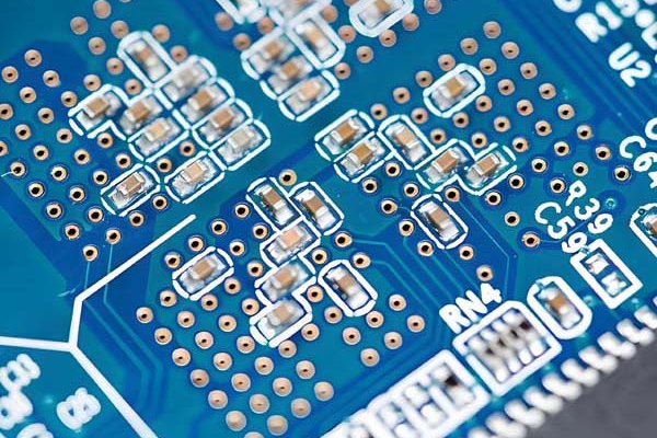
The following is an analysis of the advantages and disadvantages of mainstream PCB EDA tools and download links, which integrate industry applications, functional features, and user feedback:
—
Table of Contents
1. Altium Designer (AD)
advantage
-High usability: The interface is intuitive and supports Chinese menus, making it suitable for beginners to quickly get started.
-Full process integration: from schematic design, simulation to PCB layout and wiring integration, supporting 3D preview for collaborative structural design.
-Abundant educational resources: Widely used by universities, with numerous supporting tutorials and open-source projects.
disadvantage
-High resource consumption: High requirements for computer configuration, insufficient performance when handling complex boards with more than 12 layers.
-Functional limitations: Weak high-speed signal processing and rule management, not suitable for high-frequency or high-density design.
Download
-Official website: https://www.altium.com/
-The trial version can be applied for through the official website, and the price of the genuine version is relatively high (about $10000 per year).

—
2. Cadence Allegro
advantage
-Industry benchmark: 60% of global computer motherboards and 40% of mobile phone motherboards are designed and used, supporting high-speed, high-density, and RF design.
-Strict rule management: The Constraint Manager has powerful functions to ensure design reliability.
disadvantage
-The learning curve is steep: the interface is complex, the creation of encapsulation libraries is cumbersome, and it needs to adapt to non Chinese environments.
-High cost: Genuine licensing fees far exceed other tools, making it suitable for large enterprises.
Download
-Official website: https://www.cadence.com/
-Contact sales for trial or purchase plans.
—
3. Mentor PADS
advantage
-High cost-effectiveness: Suitable for the consumer electronics field, with high efficiency in low to medium complexity design, and friendly official Chinese support.
-Modular design: divided into three parts: Logic, Layout, and Router, with clear logic.
disadvantage
-Functional limitations: Lack of built-in simulation tools, requiring integration with plugins such as HyperLynx.
-Outdated interface: User experience lags behind AD and Allegro.
Download
-Official website: https://www.mentor.com/
-Trial version application: https://eda.sw.siemens.com/en-US/pads/
—
4. JLC EDA (PCB EDA)
advantage
-Free cloud collaboration: Based on browser operation, no installation required, permanently free and supports real-time team collaboration.
-Ecological closed loop: Design files can be directly connected to Jialichuang PCB sampling and component mall, shortening the production cycle.
disadvantage
-Functional limitations: The professional version has basic functions and insufficient support for complex multi-layer board designs.
Download
-Official website: https://lceda.cn/

—
5. OrCAD
advantage
-Schematic design standard: Seamless integration with Allegro, library management tool CIS supports full lifecycle management of components.
-Powerful simulation capability: Integrated PSpice, supporting mixed signal simulation.
disadvantage
-Expensive price: The selling price in the North American market is as high as $7995, and the domestic penetration rate is low.
Download
-Official website: https://www.cadence.com/en_US/home/tools/system-design-and-verification/pcb-design-and-analysis/orcad-pcb-designer.html
—
6. Eagle(Autodesk Fusion 360)
advantage
-Lightweight and easy to use: suitable for small projects, supports cross platform (Windows/Linux/Mac).
-Low price: The personal version is free, and the professional version has an annual fee of about $500.
disadvantage
-Functional limitations: The standard version only supports 6 layers, while the professional version has a maximum of 16 layers and is not suitable for complex designs.
Download
-Official website: https://www.autodesk.com/products/eagle/overview
—
7. KiCad (open source PCB EDA)
advantage
-Completely free and open source: active community, abundant plugin and library resources.
-Cross platform support: Supports Windows, Linux, macOS, suitable for education and small projects.
disadvantage
-Lack of learning resources: Official documents are not comprehensive enough, and enterprise level support is insufficient.
Download
-Official website: https://www.kicad.org/
—
Choose Suggestions
-Novice/student: Priority should be given to choosing Altium Designer or Jialichuang EDA for low learning costs and abundant resources.
-Consumer Electronics/Small and Medium sized Enterprises: Mentor PADS offers high cost-effectiveness and is suitable for low to medium complexity designs.
-High speed/high-density design: Cadence Allegro is the industry’s preferred choice, suitable for communication and military industries.
Attention: Some tools require trial use or purchase of genuine authorization through the official website. Cracked versions pose legal risks, and it is recommended to support genuine versions. For more tool information, please refer to the above link or related forums (such as EDA365).