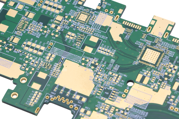
As the core carrier of electronic devices, PCB (printed circuit board) directly affects the sustainable development of the electronic industry in terms of environmental friendliness and performance. With the tightening of global environmental regulations and the increasing demand for high-performance products in the end market, halogen-free PCBs, with their green attributes and technological advantages, are becoming a key direction for industry transformation and upgrading. This article will analyze the core position of halogen-free PCB in the field of electronic manufacturing from the dimensions of its definition, environmental value, performance advantages, manufacturing process, and application scenarios.
Table of Contents
1、 Definition and Environmental Value of Halogen Free PCB
Definition and Standards
Halogen free PCB refers to a circuit board with a chlorine (Cl) and bromine (Br) content of less than 0.09% by weight, and a total of no more than 0.15% (1500ppm), in compliance with international standards JPCA-ES-01-2003 and IEC 61249-2-21. It replaces traditional halogen flame retardants with phosphorus (P) or nitrogen (N) based materials, solving the problem of halogen containing PCBs releasing toxic gases such as dioxins during combustion, significantly reducing the harm to the environment and human health.

Environmental advantages
1. Reduce toxic substance emissions: The brominated dioxins released during the combustion of traditional halogenated PCBs have strong carcinogenicity, while halogen-free PCBs use phosphorus nitrogen compounds for flame retardancy, which only generate inert gases and carbonization layers during combustion, achieving clean flame retardancy.
2. Compliance with global regulations: EU RoHS Directive, WEEE Directive, and China’s “Management Measures for Pollution Control of Electronic Information Products” strictly restrict the use of halogens, promoting halogen-free PCBs to become a necessary option for export-oriented enterprises.
3. Green production process: The halogen-free process reduces the use of halogenated chemicals, lowers the cost of wastewater and exhaust gas treatment by 30%, and meets the goal of carbon neutrality.
2、 Performance advantages and technological breakthroughs
1. Improvement of electrical performance
-Insulation Enhancement: Phosphorus nitrogen resin reduces the polarity of epoxy resin molecules, increases insulation resistance by 20% -30%, and breakdown voltage can reach 1.5 times that of traditional materials, making it suitable for high-voltage power equipment.
-Signal integrity optimization: Low dielectric constant (Dk ≤ 3.8) and dielectric loss (Df ≤ 0.005) ensure the stability of high-frequency signal transmission above 28GHz for 5G base stations.
2. Thermal stability and reliability
-Low coefficient of thermal expansion (CTE): Z-axis CTE ≤ 40ppm/℃, better matching with copper layer, reducing the risk of plated through-hole fracture caused by thermal cycling.
-High temperature resistance: Glass transition temperature (Tg) exceeding 170 ℃, able to withstand the high temperature of 260 ℃ in lead-free soldering process, suitable for automotive electronics and aerospace equipment requirements.
3. Optimization of physical properties
-Low water absorption rate: The water absorption rate is ≤ 0.1%, which is 50% lower than traditional materials, improving reliability in humid environments and extending the service life of medical equipment.
-Mechanical strength improvement: After adding inorganic fillers such as aluminum hydroxide, the bending strength is increased by 15%, making it suitable for flexible electronic and folding screen equipment.
3、 Manufacturing process and material innovation
Core process
1. Resin formula upgrade: mainly composed of phosphorus containing epoxy resin, combined with phenolic curing agent and inorganic fillers (such as silicon micro powder), balancing flame retardancy and dielectric properties.
2. Optimization of lamination process: Combining vacuum hot pressing technology with dynamic compensation system, the interlayer offset control accuracy reaches ± 25 μ m, ensuring the reliability of high-density boards with more than 20 layers.
3. Surface treatment technology: Pulse electroplating and nano coating are used to improve the uniformity of copper thickness on the pore wall by 20%, enhancing corrosion resistance and heat dissipation capabilities.

Materials Innovation
-Open fiber fiberglass cloth: improves resin permeability, solves drilling roughness problems, and increases hole wall smoothness by 30%.
-Specialized electrolytic copper foil: peel strength increased to 1.5N/mm, suitable for high-frequency and high-speed signal transmission needs.
4、 Application scenarios and market prospects
Core application areas
1. Communication equipment: 5G base stations and data centers use low loss halogen-free PCBs, reducing signal distortion by 40% and supporting data transmission of over 100Gbps.
2. Automotive Electronics: The BMS system of electric vehicles adopts metal based halogen-free PCB, which increases the thermal conductivity to 4W/m · K and improves the heat dissipation efficiency by 50%.
3. Medical equipment: Biocompatible halogen-free PCB is used for pacemakers, reducing solder joints through embedded component design and lowering the failure rate to 0.01%.
4. Consumer electronics: The thickness of the flexible halogen-free PCB for smartphones is only 0.2mm, which can be bent more than 100000 times and is compatible with foldable screens and wearable devices.
Market Trends
-Scale growth: The global halogen-free PCB market is expected to reach $3.5 billion in 2022 and surpass $5.9 billion by 2030, with a compound annual growth rate of 7.7%.
-Regional competition: The Asia Pacific region holds a 40% market share, and China has become the largest producer and consumer country with a complete industrial chain and policy support.
5、 Social Responsibility and Future Prospects
The promotion of halogen-free PCBs is not only a technological innovation, but also an important manifestation of enterprises fulfilling their ESG (environmental, social, and governance) responsibilities. Although its production cost is 15% -20% higher than traditional PCBs, in the long run, the brand premium and market access advantages brought by green manufacturing far exceed the initial investment.

In the future, with the breakthrough of AI driven intelligent production and nanomaterial technology, halogen-free PCBs will further develop towards ultra-thin and high-frequency. Enterprises need to continue investing in research and development, building a green system throughout the entire lifecycle from materials, design to recycling, in order to occupy a leading position in the global industrial chain.
Conclusion
The popularity of halogen-free PCBs marks the transformation of the electronics industry from “performance first” to “green and performance balanced”. As a PCB enterprise, deepening the cultivation of halogen-free technology is not only an inevitable choice to comply with regulations, but also a strategic measure to seize the high-end market and enhance core competitiveness. Only by driving sustainable development with innovation can we lead the industry towards a smarter and more environmentally friendly future.