-In assembled circuit boards, excessive temperatures can negatively affect the function, the components and the board itself.
Table of Contents
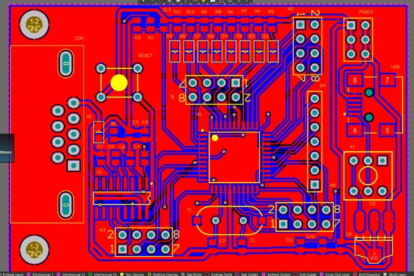
1、incorrect placement of components
Certain high-power devices need to be reserved for natural or forced ventilation to dissipate heat. Without proper airflow to dissipate heat, the PCB will accumulate most of the heat, resulting in higher temperatures, which can lead to reduced performance or damage to the circuit. Care should be taken not to place sensitive components near components that emit large amounts of heat; temperatures can be kept within safe limits through proper heat dissipation and natural or forced cooling.

2、environmental and external thermal factors
When using PCBs in extreme temperature environments, electronic components may subject to excessive stress if the temperature conditions in the target environment are not taken into account when designing PCB; generally, electronic component manufacturers provide specifications that apply within a specific temperature range.
3、 Material and thermodynamic mismatch
1. Incompatible coefficient of thermal expansion (CTE)

-Ceramic encapsulated components (CTE ≈ 6 ppm/℃) and FR-4 substrates (CTE=13-18 ppm/℃) exhibit significant differences in expansion rates during temperature cycling, leading to mechanical fatigue, delamination, or cracking of solder joints. This type of problem is particularly prominent in aerospace electronics, and CTE gradient packaging (such as Infineon SupIR-SMD) is needed to alleviate stress.
2. Insufficient thermal performance of the substrate
-The thermal conductivity of ordinary FR-4 is only 0.3 W/mK, while metal substrates (such as aluminum based) can reach 2-5 W/mK. Insufficient heat dissipation in high-power scenarios can lead to heat accumulation, and the temperature rise can exceed the device limit (such as halving the lifespan of electrolytic capacitors when they exceed 105 ℃).
3. Table: Comparison of Key Material Parameters
| Material Type | CTE (ppm/℃) | Thermal Conductivity (W/mK) | Applicable Scenarios |
| FR-4 | 13-18 | 0.3 | Consumer Electronics Low Frequency Circuit |
| Polyimide | 17-18 | 0.5 | Flexible Circuit Board |
| Aluminum substrate | 22-24 | 2-5 | LED lighting/power module |
| Ceramic Packaging | 6-7 | 20-30 | Aerospace/High Frequency Power Devices |
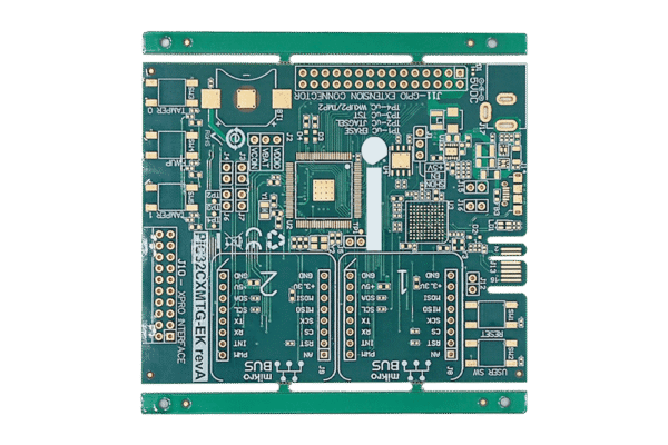
4、 Structural design and layout defects
1. Improper design of heat dissipation path
-Insufficient number or offset of heat dissipation holes (such as not directly connected below the heat source), resulting in an increase of more than 30% in thermal resistance.
-Vertical installation of PCBs hinders air convection, resulting in a 40% lower natural heat dissipation efficiency compared to horizontal installation.
2. Component layout and edge effects
-When high-speed devices (such as crystal oscillators) are close to the edge of the board, the parasitic capacitance between them and the reference ground increases, causing common mode radiation due to electric field leakage. Experiments have shown that moving the crystal oscillator inward by 1cm can reduce radiation by 15dB.
-Power layer not inwardly contracted (20H rule failure): In modern high-density PCBs, the power layer not inwardly contracted leads to increased edge resonance and a shift in radiation exceeding the standard frequency band to the GHz level.
3. Through hole and reflux path issues
-The key signal via lacks a grounding shielding hole, causing a sudden change in the return path and generating TEM waves that radiate through the board edge (such as the 48Gbps HDMI interface requiring a back drilling residual of<10mil).
-If the area of the high current circuit is too large (such as not optimizing the MOSFET drive path), the differential mode radiation intensity increases linearly with the area.

5、 Environment and work stress
1. Poor adaptability to extreme environments
-Vacuum environment (such as satellite PCB) has no air convection, and heat dissipation relies only on conduction, which can easily cause local overheating.
-The high humidity environment (>85% RH) triggers the CAF (Conductive Anode Wire) effect, which increases leakage current and thermal dissipation.
2. Thermal cycling and mechanical stress
-Sudden temperature changes (such as -55 ℃~125 ℃) accelerate CTE mismatch effects, increasing the risk of Z-direction delamination in multilayer boards by 6 times.
Solution direction and design optimization
-Thermal management: using high thermal conductivity substrates (such as metal core plates), thermal through-hole arrays (0.3mm aperture, 0.6mm spacing), and forced air cooling/liquid cooling.
-Radiation suppression: grounding via wall at the edge of the board (spacing<λ/20), power layer contraction of 40H (designed for>1GHz), crystal oscillator inward shift+copper shielding.
-Material upgrade: Low Df board (Megtron 6 Df=0.002) is selected for high-frequency applications, and CTE gradient packaging is used for aerospace components.
>Case evidence: A certain LED driver power supply exceeded the radiation standard due to the large MOSFET circuit area. After optimizing the layout and adding shielding vias, the EMI decreased by 12dB and the temperature rise decreased by 18 ℃.
Solving PCB heating and radiation problems requires collaborative optimization of electrical design, material selection, structural layout, and environmental adaptation. Especially in high-frequency, high-power, and extreme environments, it is necessary to follow the principles of “low impedance, small circuit, CTE matching, and forced heat dissipation” to suppress energy conversion and leakage from the source.