What should be paid attention to when laying out high-frequency PCBs
The application of high-frequency PCBs (printed circuit boards) is becoming increasingly widespread in fields such as 5G communication, radar systems, and high-speed data transmission. With the increase of signal frequency, issues such as loss, reflection, and crosstalk during signal transmission become increasingly prominent, making the layout design of high-frequency PCBs crucial. A reasonable layout can effectively ensure signal integrity, reduce electromagnetic interference, and improve system performance. This blog will elaborate on the key points of high-frequency PCB layout from multiple dimensions.
Table of Contents
1、 Signal integrity optimization
(1) Control signal transmission path
High frequency signals are extremely sensitive to the length of the transmission path, and excessively long wiring can increase signal delay and loss. When laying out, the routing length of key high-frequency signals should be shortened as much as possible to avoid detours and detours. For clock signals, RF signals, etc., a “short and straight” wiring strategy should be adopted. At the same time, it is necessary to strictly control the bending angle of the wiring, avoid right or sharp angles, and prevent signal reflection. It is recommended to use a 45 ° or circular arc transition.

(2) Impedance matching design
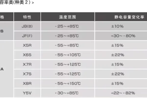
High frequency signal transmission requires ensuring that the line impedance matches the impedance of the signal source and load to reduce signal reflection. Before layout, the target impedance (usually 50 Ω or 75 Ω) needs to be calculated based on parameters such as signal frequency and dielectric constant of the board. Impedance control is achieved by adjusting the wire width, dielectric thickness, and other methods. In addition, attention should be paid to the continuity of impedance at connectors, vias, and other locations to avoid impedance mutations.
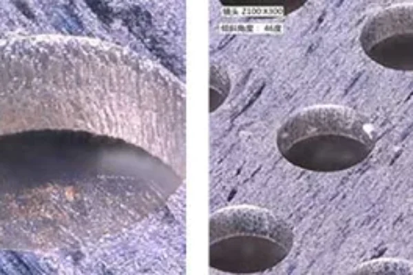
(3) Reduce the use of vias
Vias can introduce parasitic capacitance and inductance, causing interference to high-frequency signals. Therefore, the number of vias on high-frequency signal traces should be minimized as much as possible. If it is necessary to use vias, priority should be given to smaller sized micropores and the layout of vias should be optimized to avoid multiple vias being arranged in a concentrated manner and reduce the influence of parasitic parameters.
2、 Electromagnetic Compatibility (EMC) Design
(1) Reasonable zoning layout
Physically isolate the high-frequency signal area, low-frequency signal area, and power supply area to reduce mutual interference between signals of different frequencies. The high-frequency signal area should be kept away from analog circuits and sensitive components that are susceptible to interference; Maintain a certain distance between the power module and the signal line to prevent power noise from coupling into the signal path. Each functional area can be further isolated by grounding isolation tape or shielding wall.
(2) Shielding and grounding design

Shielding treatment can be applied to high-frequency signal wiring and key components (such as RF chips and crystal oscillators) using metal shielding covers or copper shielding. Meanwhile, building a good grounding system is the key to suppressing electromagnetic interference. High frequency PCBs should use large-area copper cladding as the grounding plane to ensure a short and wide grounding path and reduce grounding impedance. The grounding wires of different functional modules should be designed independently to avoid forming grounding loops and prevent the generation and propagation of electromagnetic interference.
(3) Filtering and decoupling design
Reasonably place filtering capacitors, inductors, and other components at the power input port and key signal nodes to filter out high-frequency noise. For power lines, a multi-stage filtering circuit is used to suppress power ripple; Configure appropriate decoupling capacitors for the power pins of each chip to reduce the impact of power noise on the chip. When laying out, filtering components should be placed as close as possible to the protected components or circuits to improve the filtering effect.
3、 Component layout optimization
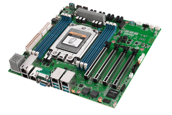
(1) Location selection of key components
The layout of high-frequency components (such as RF devices and high-speed connectors) directly affects signal performance. Place it near the edge or interface of the circuit board to shorten the input and output path of the signal. As the source of high-frequency signals, crystal oscillators should be kept away from interference sources and as close as possible to the chip using the clock signal to reduce transmission delay and interference of the clock signal.
(2) Component spacing control
To avoid electromagnetic coupling and crosstalk between components, it is necessary to ensure sufficient spacing between the components. The spacing between high-frequency components and other components should be appropriately increased according to the signal frequency and power; For high-frequency signal lines running side by side, the principle of 3W (line spacing of at least 3 times the line width) should be met to reduce crosstalk between lines.
(3) Heat dissipation design considerations
When high-frequency circuits work, the components generate a large amount of heat, and a reasonable heat dissipation design can ensure stable operation of the components. When laying out, place components with high heat generation, such as power amplifiers and power chips, in locations that are conducive to heat dissipation, such as near ventilation openings or heat sink installation areas. At the same time, the heat dissipation capability of the circuit board can be improved by increasing heat dissipation through holes and optimizing the copper coating area.
The above content systematically summarizes the core points of high-frequency PCB layout. If you would like to learn more about specific cases or special requirements for high-frequency PCB layout in different industries, please feel free to contact me at any time.
Get your exclusive quote immediately: fill out the form or send an email directly.As a professional PCB manufacturer for hobbyist , we will provide you with a quote service within 24 hours. Enjoy free DFM optimization and a 10% discount on SMT patches for your first order!