Table of Contents
Analysis of QFN package features: The Core Solution for High Density PCB Design
>Reducing volume by 84% and improving thermal performance by 55% – QFN packaging, with its revolutionary pinless design, is becoming the preferred packaging solution for smartphones, automotive electronics, and IoT devices.
In the wave of continuous miniaturization and high performance of electronic devices, QFN (Quad Flat No led Package) has become a benchmark technology for replacing traditional TSOP and PLCC packaging due to its three characteristics of small space occupation, high heat dissipation efficiency, and excellent electrical performance. According to QYResearch data, the global QFN packaging market size has reached 1.452 billion US dollars in 2024, and is expected to exceed 1.894 billion US dollars by 2031, with a compound annual growth rate of 3.9%. This blog will delve into the technical characteristics, application practices, and future trends of QFN packaging, providing key references for PCB design and manufacturing.
1、QFN package features Basic Concept: Redefining High Density Interconnection
QFN is a surface mount package without pins, and its core structure consists of two major elements:
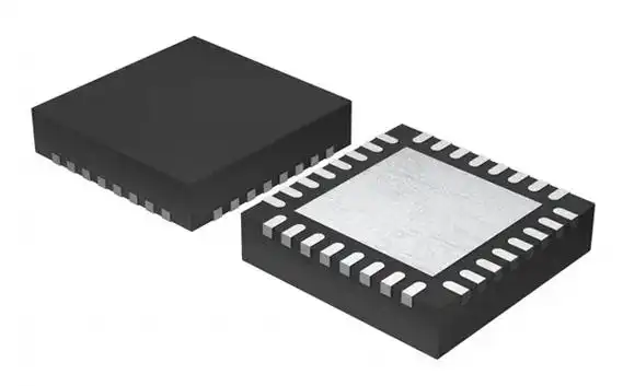
-Peripheral electrical pads: Encapsulated with electrode contacts on all four sides, directly connected to PCB pads, replacing traditional gull wing shaped pins.
-Central exposed heat dissipation pad: The bottom large-area metal pad is directly connected to the PCB ground layer through thermal conductive vias, forming an efficient heat dissipation channel.
Compared to the 28 pin PLCC package, the 32 pin QFN can achieve:
-84% reduction in area (5mm × 5mm)
-Thickness reduced by 80% (0.9mm)
-Weight reduced by 95% (0.06g)
-Parasitic effect reduced by 50%
2、 QFN package features
1. Ultimate space utilization rate
-Pin spacing refinement: Supports spacing of 0.4mm, 0.5mm, 0.65mm, etc., with a size reduction of 62% compared to TSSOP packaging under the same function.
-Ultra thin design: The packaging thickness is only 0.45-0.9mm, meeting the miniaturization needs of wearable devices and medical sensors.

2. Excellent electrical performance
-Ultra low impedance path: The pinless design shortens the conductive path, reduces self inductance by 60%, reduces capacitance interference by 30%, and supports high-frequency signal transmission (>10GHz).
-Signal integrity assurance: Short path reduces signal attenuation, suitable for 5G RF front-end and high-speed data converters.
3. Efficient thermal management capability
-Central heat dissipation pad+via matrix: Heat is directly conducted to the PCB ground layer, which increases the heat dissipation efficiency by 55% compared to TSSOP packaging.
-Automotive grade heat dissipation solution: Combined with aluminum substrate and 2oz thick copper foil, it can support a power density of 100W+for electric vehicle OBC modules.
4. Lightweight and cost advantages
-The cost of plastic packaging (epoxy resin based) is 30% lower than that of ceramic QFN, and it is suitable for reflow soldering process.
–Copper wire bonding technology further reduces material costs and is suitable for mass production of consumer electronics.
3、 Challenge and Solution: Breaking through Manufacturing Bottlenecks
1. Poor soldering on the side
-Industry pain point: Insufficient solder climb caused by oxidation of QFN side pads. IPC-A-610 Level 3 standard requires a solder climb height of 50% of the pad, but the actual yield rate is only 60-70%.
-Innovative solutions:
-Optimization of steel mesh opening: adopting an internal cutting and external pulling design, increasing the amount of solder paste and reducing bridging.
-High activity solder paste: Xinfujin anti gravity climbing solder paste enhances the wettability of oxidized surfaces.
-Vacuum reflow soldering: reduces oxygen residue and improves welding yield to 98%.
2. Difficulties in repair and testing
-X-ray fluoroscopy detection: Identify bottom solder joint virtual welding (the main cause of industry yield loss) through 3D X-ray.
-Laser local heating repair: precise temperature control to avoid damage to surrounding components, reducing repair costs by 40%.
3. Test interface reliability
-High frequency testing challenge: RF signals above 20GHz require a socket contact resistance of<10m Ω for testing.
-Joule 20 Test Plan:
-Single piece contact structure reduces inductance and supports temperature range of -40 ° C~+125 ° C
-The plug-in life is 500000 times, and the PCB pad wear rate has decreased by 90%.
4、 Application case analysis: Multi domain validation of reliability
1. Smart speaker audio decoding chip (Ruixin Micro solution)
-The advantages of QFN are reflected in:
-0.9mm thickness suitable for compact cavity design
-Low impedance ensures 96dB signal-to-noise ratio audio output
-Bottom heat dissipation pads solve the problem of temperature rise in enclosed spaces.
2. Industrial temperature sensors
-Strict environmental verification:
-Anti electromagnetic interference design with an error rate of less than 0.001% in motor control cabinets
-The working temperature range of -40 ℃~125 ℃ has been certified by IATF 16949.
3. Electric vehicle OBC module
-High power density design:
-12 × 12mm large-sized QFN with 6 rows of pins (156Pin)
-Copper wire bonding+2oz copper foil carrying 30A current, temperature rise<15 ℃.
5、 Future Development Trend: Breakthrough in Materials and Integration Technology
1. High frequency material adaptation
-LCP liquid crystal polymer substrate: solves the signal loss in the 5G millimeter wave frequency band. The dielectric constant of PTFE material is reduced to 2.2, and the loss is 60% lower than FR-4.
2. High density integrated innovation
-Multi row pin design: Changdian Technology’s QFNs mr technology achieves a pin count of 156+and a 40% increase in area utilization.
-Stacked QFN: vertically interconnected power layer and control layer, with a power density exceeding 10W/cm ³.
3. Restructuring of Global Supply Chain
-Tariff response strategy:
-Southeast Asian production capacity layout (Vietnamese factory undertakes European and American orders, avoiding 25% tariffs).
-Localized material procurement: China’s copper foil production capacity accounts for 65% of the world’s total, reducing the risk of substrate cost fluctuations.
Conclusion: Empowering the Core Packaging Technology of Next Generation Electronic Systems
As the penetration rate of AIoT devices increases and the complexity of automotive electronics upgrades, QFN packaging will continue to evolve towards ultra-high frequency, ultra-thin, and high pin count.
SysPCB as a PCB manufacturing enterprise, we offer:
-QFN specialized sheet solution: one-stop supply of high Tg FR-4, metal substrate, and high-frequency PTFE substrate
-DFM Collaborative Design: Optimizing Solder Crawling and Heat Dissipation Via Solutions Based on Million level Case Library
-Quick sampling service: 24-hour delivery of QFN samples, supporting X-RAY full inspection.
Get your exclusive quote immediately: fill out the form or send an email directly, and we will provide you with a quote service within 24 hours. Enjoy free DFM optimization and a 10% discount on SMT patches for your first order!