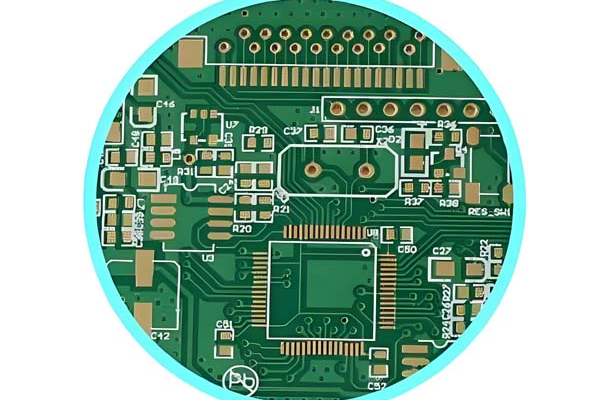
In PCB (printed circuit board) design, the “golden rule” usually refers to key design principles based on engineering practice to ensure the electrical performance, reliability, and manufacturability of the circuit board. The following are 5 widely recognized core design principles in the industry, with detailed explanations and application scenarios:
Table of Contents
1、 Signal integrity design: Control wiring impedance and delay
Core Requirements
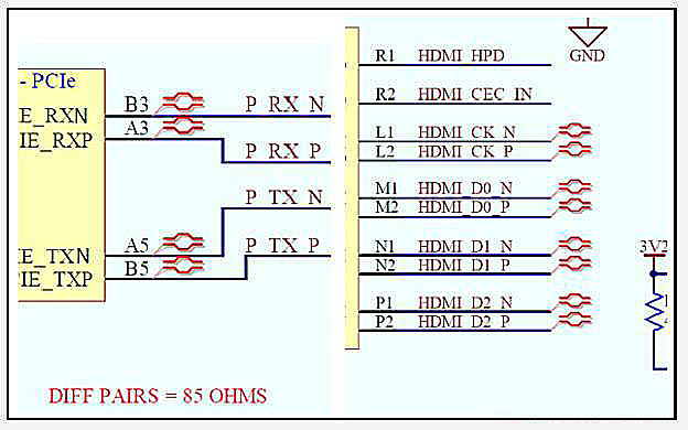
–Impedance matching: High speed signal lines (such as USB, HDMI, PCIe) need to control their characteristic impedance according to specifications (commonly 50 Ω/differential 100 Ω), which can be calculated based on the wire width, dielectric thickness, and copper foil thickness (using tools such as SI9000).
-Wire length matching: Parallel buses (such as DDR) need to control equal length errors (usually ≤ 5ml) to avoid data errors caused by timing offset.
-Example: The address/data line from CPU to memory needs to be length matched according to the topology structure (T-shaped or star shaped), and an error of more than 10 mil may cause signal reflection.
extended technique
-Avoid right angle wiring (which can easily cause reflection) and use a 45 ° corner or arc instead; Keep the high-speed line away from the edge of the PCB (to reduce EMI radiation).
2、 Power and ground plane design: layering and decoupling
Core principles
-Power/ground plane layering: The dedicated power layer in the multi-layer board is adjacent to the ground layer, and the capacitance effect is used to reduce power noise. The closer the interlayer distance, the better the decoupling effect (recommended ≤ 5ml).
-Decoupling capacitor layout: At least one 10 μ F electrolytic capacitor and one 0.1 μ F ceramic capacitor should be configured for every 10 ICs, and the capacitors should be close to the chip power pins (with a wire length of less than 0.1 inches).
-Segmentation strategy: Multiple voltage domains need to divide the power plane to avoid interference from different voltages. The segmentation lines need to overlap with the ground plane and be far away from high-speed signal lines.
Layer stackup strategies:
| Layer | Function | Material | Key Parameter |
| L1 | Critical signals | Rogers 4350B | Df=0.0037 @10GHz |
| L2 | Solid ground | FR4 | Impedance Δ≤5% |
| L3 | Power (split planes) | FR4 | Z<sub>target</sub>≤50mΩ |
| L6 | Ground | FR4 | 100% coverage |
PDN design essentials:
– Target impedance: Calculate Z<sub>target</sub> = (V<sub>ripple</sub> × Duty)/ΔI (e.g., 1.8V/50mV/1A → 50mΩ).
– Capacitor placement: Position 0.1μF ceramics ≤3mm from IC pins; use 10μF tantalum at power inputs.
– Via stitching: Place ground vias ≤λ/20 spacing (e.g., 1mm at 6GHz) around noisy zones.
Case
-The digital power supply and analog power supply in the industrial control board need to be strictly separated, otherwise the ADC sampling accuracy may decrease by more than 10%.
3、 EMC (Electromagnetic Compatibility) Design: Suppressing Interference and Resisting Interference
Key measures
-Wiring shielding: Sensitive signal lines (such as audio and sensor signals) need to be surrounded by ground wires or kept at a distance of 3W (three times the line width) from the power line.
-Crystal oscillator processing: The crystal oscillator shell is grounded, and a grounding copper skin is laid around it to avoid getting close to the I/O interface (to prevent interference and leakage).
-PCB edge processing: The I/O interface needs to be equipped with ESD protection devices, and the interface ground should be connected to the internal digital ground through a 0 Ω resistor or magnetic beads to prevent electrostatic breakdown.
4、 Thermal management design: heat dissipation path and layout
Design points
-Heat source layout: High power devices (such as power ICs and resistors) should be placed in a dispersed manner to avoid concentrated heating; Reserve sufficient space in the installation area of the radiator to avoid obstruction by wiring or components.
-Heat dissipation copper skin: Multiple layers of heat dissipation are connected through large-area copper foil and via holes (VIA), with a via density of ≥ 10/mm ², which can improve heat dissipation efficiency by more than 30%.
-Material selection: High power PCBs can use FR-4 TG170 or aluminum substrates, with thermal conductivity 2-5 times higher than ordinary FR-4.
Application scenarios
-The MOSFET in the power board needs to be directly soldered onto the copper sheet, with a copper sheet area of ≥ 100mm ² and more than 10 through holes drilled.
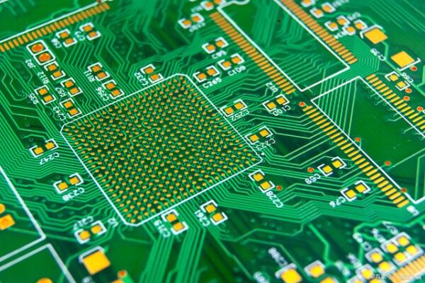
5、 Manufacturability and Maintainability: DFM and DFA Principles
Specific specifications
-Wire spacing: For ordinary PCBs, the line width/spacing should be ≥ 5mil, while for high-density boards (HDI), it can reach 3mil, but it is necessary to ensure the factory’s process capability (such as line width tolerance ± 1mil).
-Solder pad design: SMD solder pads have a length of 0.2mm longer than the component pins and a consistent width; The diameter of BGA solder pads needs to be calculated based on the ball diameter (e.g. 0.5mm ball diameter corresponds to 0.35mm solder pads).
-Test point reservation: Each PCB must be equipped with at least 4 grounding test points, with a spacing of ≤ 150mm, to facilitate AOI inspection and maintenance.
Avoiding Misunderstandings
-Do not place vias under BGA, otherwise it may cause solder ball voids; The distance between the plug-in hole and the solder pad is ≥ 1mm to prevent deformation during welding.
Attachment: PCB Design Golden Rule Quick Reference Table
| Rules | Core Requirements | Typical Parameters | Risk of Violation |
| Signal integrity | Impedance matching, equal length control | 50 Ω single ended/100 Ω differential, error ≤ 5mil | Signal reflection, timing error |
| Power supply ground plane | Layered decoupling, capacitor layout | Capacitor distance from pin<0.1 inches | Large power ripple, abnormal IC operation |
| EMC design | 3W principle, grounding shielding | The distance between signal lines and power lines is ≥ 3 times the line width | Radiation exceeds the standard, poor anti-interference ability |
| Thermal management | Copper skin heat dissipation, heat source dispersion | Via density ≥ 10/mm ² | Component overheating failure |
| Manufacturability | line width spacing, reserved test points | ordinary board line width ≥ 5ml | low production yield, difficult maintenance |
Extended suggestions
-Tool assistance: Use the rule checking function (DRC) of software such as Altium Designer and PADS to verify in real-time whether the design complies with the rules;
-Industry standards: Refer to IPC-2221 (PCB Design Specification) and JEDEC (Semiconductor Packaging Standard), adjust design parameters according to product type (consumer electronics/automotive electronics).
Following the above rules can significantly reduce the iteration cost of PCB design, especially in high-speed and high reliability scenarios, which is the key to ensuring the success of product production in one go.
→ [Download High-Density PCB Checklist]
Includes impedance calculators, thermal via specs, and DFM audit templates