As the cornerstone of electronic interconnect technology, wire bonding occupies a core position in the semiconductor packaging field due to its high flexibility, low cost, and mature reliability. With the continuous improvement of integration requirements for 5G communication, automotive electronics, and high-performance computing, innovation in wire bonding technology and collaborative design of PCB substrates are becoming the key to industry competition. This article will deeply analyze the technological context and future trends of wire bonding PCB from the dimensions of technical principles, material evolution, process breakthroughs, and PCB collaborative innovation.
Table of Contents
1、 Technical Principles: Scientific Game of Three Bonding Methods
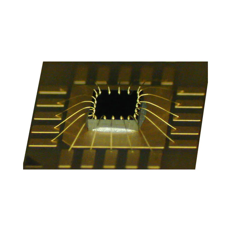
Wire bonding connects chip bond pads and substrate pads through metal wires to achieve electrical signal transmission. The core process is divided into three categories based on the energy loading method:
1. Ultrasonic bonding
Using 20-60kHz ultrasonic waves to rub metal leads (such as aluminum wires) against the surface of solder pads, damaging the oxide layer and causing plastic deformation, achieving atomic level diffusion bonding. No heating required, suitable for temperature sensitive flexible substrates, but sensitive to pad thickness (≥ 0.6 μ m), prone to causing “Crater Cracks”.
2. Hot press bonding
Press the molten metal ball (such as gold wire) onto the solder pad under pressure at a high temperature of 150-250 ℃. The ball size is 2-3 times the diameter of the wire, with high bonding strength, but high temperature can easily cause warping of the polymer substrate.
3. Thermal ultrasonic bonding (mainstream process)
By combining ultrasound with low-temperature heating at 100-150 ℃, the growth of intermetallic compounds (IMC) is inhibited while enhancing bonding strength. High frequency vibration welding of gold/copper wire balls, suitable for high-density BGA packaging, with a yield rate of up to 99.95%.
>Bonding process: solder ball forming → first solder joint bonding (chip pad) → wire arc forming → second solder joint bonding (substrate pad) → wire cutting.
2、 Material Innovation: The Ultimate Challenge of Wire Performance
The selection of bonding wire directly determines the electrical performance and reliability. The comparison of mainstream material characteristics is as follows:
| Wire type | Diameter range (μ m) | Electrical resistivity (Ω· m) | Thermal conductivity (W/m · K) | Core advantages | Applicable scenarios |
| gold thread | 15-50 | 2.20 | 320 | Strong antioxidant properties and high HAST reliability | Aerospace and military components |
| copper wire | 18-50 | 1.72 | 400 | Low cost, low resistivity | Consumer Electronics Framework Packaging |
| Palladium plated copper wire | 18-30 | 1.75 | 390 | Excellent corrosion resistance, with a storage period of 7 days | Substrate high-frequency packaging |
| Silver alloy wire | 16-75 | 1.63 | 430 | Low cost, good scalability | LED and medium low speed substrate packaging |

Technical pain points and breakthroughs:
-Copper wire challenge: High hardness can easily cause surface cracks, requiring nitrogen hydrogen mixed gas shielded welding;
-IMC failure: Kirkendall Voids are easily generated at the gold aluminum interface, and diffusion can be suppressed by using a palladium plating layer;
-Ultra fine wire diameter: 20 μ m copper wire bonding has achieved a pitch of 4 μ m, suitable for high-density interconnection of AI chips.
3、 Technological breakthrough: dual upgrade of precision and reliability
1. Segmented bonding technology
For brittle chip pads, a two-stage ultrasonic loading method of “low-frequency pre soldering+high-frequency strengthening” is adopted:
-The first paragraph: Pre weld with low-frequency ultrasound (0.4-0.7 times the conventional frequency) for 25ms to preliminarily damage the oxide layer;
-Second paragraph: High frequency ultrasonic short-term loading (<15ms) deepens atomic diffusion, increases solder joint strength by 40%, and reduces crater crack rate by 60%.
2. Wafer level bonding film (DAF)
Replacing traditional epoxy resin silver paste, DAF film thickness can be controlled to the micrometer level, and the coefficient of thermal expansion (CTE) matches the chip and substrate, reducing the warpage of multi-layer chip stacking from 0.5% to 0.1%, promoting the integration revolution of multi chip packaging (MCP).
3. Intelligent process monitoring
The AOI system detects the morphology of solder joints in real time, and combines MIL-STD-883 standard to perform Pull Test and Shear Test, achieving zero defect control.
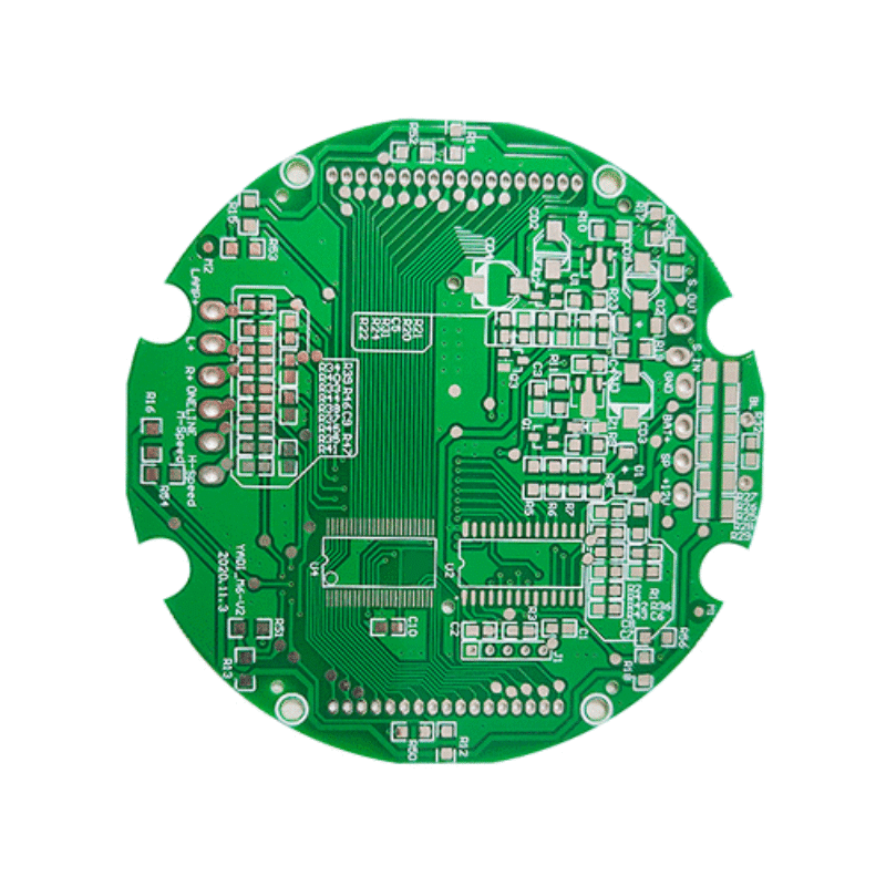
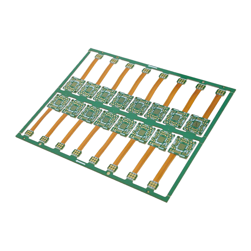
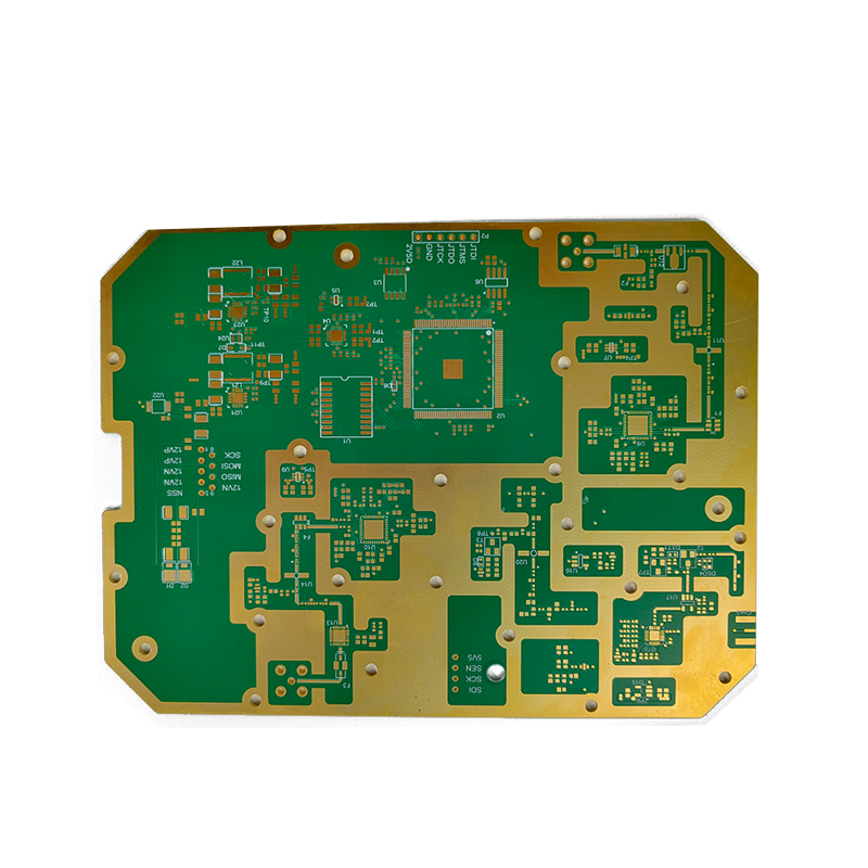
4、 PCB Collaborative Design: The Core Empowerment of Substrate Technology
As the carrier of the bonding process, the design of the PCB substrate directly determines the signal integrity and heat dissipation efficiency:
1. Micro refinement design of solder pads
-Pad size ≥ 1.5 times the diameter of the bonding ball, with a 15 μ m clearance area reserved at the edge to prevent short circuits;
-The ceramic antenna substrate uses window opening fiberglass cloth to improve resin permeability and reduce hole wall roughness by 30%.
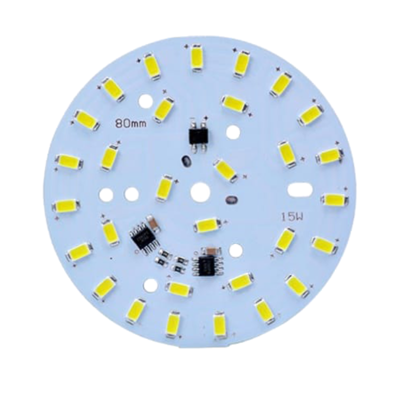
2. Thermal management architecture
-The thermal conductivity of the metal substrate (aluminum/copper) is 2-4W/m · K, which is 4 times higher than FR-4 and solves local hotspots in BGA packaging;
-The BMS system of electric vehicles adopts aluminum substrate+copper wire bonding, which improves the heat dissipation efficiency by 50%.
3. EDA toolchain integration
Altium Designer supports 3D modeling of bonding wires, which can define wire arc height, diameter, and bonding finger orientation. DRC rules verify the minimum wire spacing and length to avoid high-frequency signal crosstalk.
5、 Application Trend: Dual track Evolution of High Frequency and Green Manufacturing
1. High frequency communication scenarios
The 28GHz RF module of the 5G base station adopts a low loss substrate (Df ≤ 0.003) and gold wire bonding, reducing the signal attenuation rate by 40%; The satellite communication PCB is matched with Z-axis CTE (≤ 8ppm/℃) and can withstand temperature difference cycles of -55 ℃~250 ℃.
2. Green manufacturing transformation
-Halogen free solder mask ink: ion migration rate reduced by 50%, compliant with RoHS directive;
-Closed loop circulation of etching solution: Copper recovery rate>90%, reducing the cost of hazardous waste treatment.
3. AI driven smart factory
Machine learning algorithms predict bonding parameters, dynamically optimize ultrasound energy and pressure, increase yield to 99.98%, and reduce energy consumption by 20%.
Conclusion
Wire bonding is not only a technological inheritance of packaging technology, but also a strategic pivot for the integration and innovation of PCB and semiconductor. From the material revolution of copper wire replacing gold wire, to the precision leap of segmented bonding, every breakthrough profoundly reshapes the reliability boundary of electronic manufacturing. As a PCB enterprise, we are committed to substrate chip collaborative design, high-frequency material research and development, and deep integration of intelligent chemical process chains, providing global customers with full scenario bonding solutions from consumer electronics to aerospace grade devices. When Moore’s Law approaches the physical limit, only underlying innovation can connect the infinite future.