Introduction
The PCI-SIG (Peripheral Component Interconnect Special Interest Group) has officially released the PCIe 7.0 specification in June 2025, marking a groundbreaking advancement in high-speed interconnect technology. With a raw data rate of 128 GT/s per lane and a bidirectional bandwidth of 512 GB/s in x16 configurations, PCIe 7.0 is set to revolutionize data-intensive applications such as AI/ML, data centers, quantum computing, and 800G Ethernet. For PCB enterprises, this evolution presents both opportunities and challenges in designing boards that meet the stringent demands of next-generation hardware. This article explores the key features of PCIe 7.0, its impact on PCB design, and how your business can stay ahead of the curve.
Table of Contents
1. Key Features of PCIe 7.0
Unprecedented Bandwidth and Speed
•128 GT/s per Lane: PCIe 7.0 doubles the data rate of PCIe 6.0 (64 GT/s), enabling a bidirectional bandwidth of 512 GB/s in x16 configurations. This means a PCIe 7.0 x4 slot can match the bandwidth of a PCIe 5.0 x16 slot.
•PAM4 Signaling and FLIT Encoding: Like PCIe 6.0, PCIe 7.0 uses PAM4 (Pulse Amplitude Modulation 4-level) signaling and FLIT (Flow Control Unit)-based encoding to maximize data density per clock cycle. However, it introduces optimizations for signal integrity and error correction at higher frequencies.
Enhanced Power Efficiency
•PCIe 7.0 achieves higher energy efficiency through reduced signaling voltage swings and refined power management states (e.g., L0p/L1 sub-states), critical for power-sensitive applications like AI accelerators and high-performance computing (HPC).
Backward Compatibility
•The specification maintains full backward compatibility with previous PCIe generations (1.0–6.0), ensuring seamless integration into existing infrastructure.
Optical Interconnect Support
•A landmark addition is the “Optical Aware Retimer” Engineering Change Notice (ECN), which standardizes PCIe over fiber optics. This enables long-distance connections (e.g., between server racks) with minimal signal loss, leveraging technologies like active optical cables (AOCs) and co-packaged optics (CPO).
2. Applications of PCIe 7.0
•AI/ML and HPC: Supports massive data throughput for GPU/NPU clusters and AI training workloads.
•Data Centers: Facilitates 800G Ethernet and hyper-scale cloud infrastructure.
•Quantum Computing: Provides low-latency interconnects for quantum hardware.
•Automotive and Aerospace: Meets the needs of advanced driver-assistance systems (ADAS) and avionics.
3. PCB Design Challenges and Solutions
Integrating PCIe 7.0 into PCBs requires addressing signal integrity, thermal management, and power delivery with unprecedented precision.
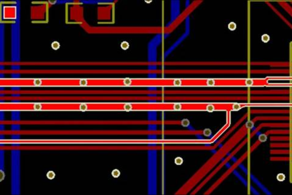
Signal Integrity
•Higher Frequency Demands: PCIe 7.0 operates at a 32 GHz Nyquist frequency (double that of PCIe 6.0), necessitating strict impedance control (85Ω differential pairs), low-loss dielectric materials (e.g., Rogers substrates), and advanced EMI shielding.
•Loss Budget Management: The end-to-end channel loss budget is capped at -36 dB (die-to-die). PCB designers must minimize insertion loss through optimized trace layouts and use of retimers.
•Equalization Techniques: PCIe 7.0 replaces 16-tap DFE with 1-tap DFE and 29-tap FFE for improved signal recovery.
Thermal Management
•Heat Dissipation: Higher data rates increase power density. Use thermal vias, copper pours, and heatsinks to manage hotspots.
•Component Placement: Separate high-power components (e.g., controllers, SerDes) from sensitive analog circuits.
Power Integrity
•Stable Power Delivery: Implement multi-phase voltage regulators and decoupling capacitors to suppress noise.
•Efficiency Optimization: Leverage dynamic power scaling (e.g., L0p mode) to reduce power during idle states.
Connector and Material Selection
•High-Speed Connectors: Use PCIe 7.0-certified connectors (e.g., Amphenol’s Mini Cool Edge IO) with tighter tolerances, improved shielding, and advanced contact materials to minimize crosstalk.
•Low-Loss Materials: Adopt substrates with Dk < 3.5 and Df < 0.005 at 32 GHz to reduce signal attenuation.
4. Industry Outlook and Readiness
•Market Timeline: PCI-SIG expects the first PCIe 7.0 devices to hit the market by 2027–2028.
•Optical Integration: Optical PCIe solutions will initially deploy in data centers for AI workloads, with broader adoption in HPC and networking.
•Collaborations: PCB enterprises should partner with connector suppliers (e.g., TE Connectivity, Samtec) and semiconductor players to co-optimize designs.
5. How PCB Enterprises Can Prepare
•Invest in R&D: Develop expertise in high-frequency simulation tools (e.g., ANSYS HFSS) and multilayer PCB stacking techniques.
•Adopt Standards: Ensure compliance with IPC-6012 and PCI-SIG specifications for reliability.
•Focus on Training: Educate design teams on PCIe 7.0’s electrical requirements and optical interconnect fundamentals.
Conclusion
PCIe 7.0 is not merely an incremental update but a transformative leap in interconnect technology. For PCB enterprises, mastering its design intricacies—signal integrity, thermal management, and optical integration—will be crucial for capturing opportunities in AI, data centers, and beyond. By embracing advanced materials, simulation tools, and industry collaborations, your business can lead the charge into the terabyte-speed era.
Get your exclusive quote immediately: fill out the form or send an email directly.As a professional PCB manufacturer for hobbyist , we will provide you with a quote service within 24 hours. Enjoy free DFM optimization and a 10% discount on SMT patches for your first order!