In today’s rapidly evolving electronics landscape, PCB reverse engineering is often misunderstood as mere “cloning” or “counterfeiting.” This perspective is not only simplistic but obscures its true value: The essence of PCB reverse engineering is never imitation—it is deep analysis, learning, and ultimately, transcendence.
Table of Contents
Ⅰ.Reverse Decoding: A Microscope for Design Intelligence
PCB reverse engineering is a precise technical decoding process:
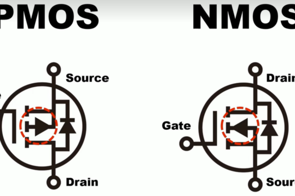
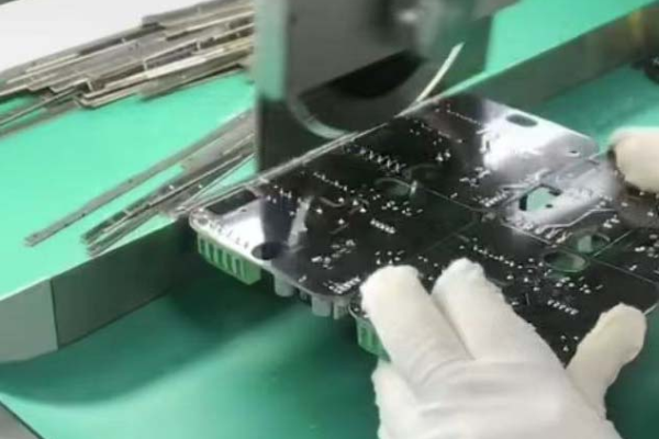
1. Physical Structure Dissection: Utilizes techniques like layer-by-layer scanning and image processing to accurately reconstruct PCB physical layout, layer stackup, and trace routing.
2. Component Information Extraction: Identifies component models, specifications, and parameters to build a complete Bill of Materials (BOM).
3. Schematic Reconstruction: Deduces the logical architecture and signal flow of the circuit design based on physical connection relationships.
This process itself is a profound deconstruction of the original designer’s thought process.
Ⅱ.Purpose Elevated: Learning and Breakthroughs on the Shoulders of Giants
The ultimate significance of PCB reverse engineering lies in Learning, Absorption, and Re-innovation:
* Learning Cutting-Edge Technology: Top-tier international products often embody the latest circuit design concepts, high-frequency/high-speed signal handling techniques, high-density integration solutions, and advanced thermal/EMC/EMI management. Reverse engineering provides the most direct key to unlocking this technological treasure trove, allowing close examination of their intricacies.
* Deciphering Design Essence: Why was this topology chosen? How does this filter network achieve exceptional noise suppression? What’s the reasoning behind this power plane segmentation? Reverse engineering enables engineers to deeply understand the underlying physics and engineering trade-offs, absorbing the design philosophy and best practices.
* Grasping Core Know-How: Critical design techniques and tacit knowledge (e.g., specific component selection rationale, critical signal routing constraints, application of special processes) are rarely found in public documentation. Reverse engineering offers invaluable insight into this “hidden knowledge.”
* Avoiding Design Pitfalls: Analyzing mature products helps understand past mistakes (“traps”), preventing their repetition in original designs and accelerating development.
Ⅲ.Beyond Imitation: Innovation Empowered by Reverse Engineering
The end goal of learning is not replication, but sparking original design and differentiated innovation:
1. Localization Optimization & Enhancement: Deep understanding allows optimization for specific market needs, cost constraints, or performance requirements. Examples: improving power efficiency, enhancing interface compatibility, boosting reliability in specific environments, or adopting superior domestic alternatives.
2. Modular Adoption & Integration: Master key functional modules (e.g., sophisticated clock circuits, efficient DC-DC converters, low-noise front-end acquisition circuits) from excellent designs and integrate them as reliable building blocks into new product designs.
3. Springboard for Secondary Innovation: Armed with core principles and design thinking, engineers can leap beyond the original framework. By incorporating new trends (e.g., SiP, advanced processors, AI algorithms), they develop products with superior functionality, higher integration, and enhanced user experience.
4. Bridge to Close the Technology Gap: For those catching up, PCB reverse engineering is an efficient means to rapidly learn advanced design methodologies and compensate for experience gaps, paving the way for full-fledged independent innovation.
Case Study: A domestic team analyzed the PCB design of a high-end international industrial controller. They gained deep insights into its complex backplane high-speed signal integrity and ruggedized reliability design. Not only did they significantly improve the signal transmission performance of their own product, but they also achieved breakthroughs in thermal and shock resistance design. The result was a next-generation controller better suited to demanding local industrial environments, offering competitive cost advantages, successfully achieving market substitution.
Ⅳ.Navigating Legal and Ethical Boundaries
A crucial emphasis: Legality and compliance are prerequisites for PCB reverse engineering as a learning tool.
* Respect Intellectual Property (IP): Learning and referencing ≠ illegal copying and selling. The core lies in mastering design concepts and technical principles, not direct product piracy for profit.
* Legitimate Purposes: Reverse engineering for interoperability research, education, or analyzing design concepts (without directly copying the product) may be considered “fair use” within specific legal frameworks.
* Innovation-Driven: The ultimate objective must always be original design, improvement, and the creation of products with independent IP.
Ⅴ.Conclusion: The Innovation Cycle – From Reverse to Forward
PCB reverse engineering is not the destination; it is the starting point for technological evolution. It provides a shortcut to deeply understand the world’s leading electronic design wisdom. When undertaken with the tenets of learning, absorption, and re-innovation, PCB reverse engineering transforms from a simple “copying” tool into a powerful engine for technological breakthroughs and product innovation. Only by internalizing the knowledge gained through reverse engineering and boldly applying it to uncharted innovative territory can we truly achieve “surpassing the master,” propelling the domestic electronics industry ever upward. Every dissection of an exceptional design fuels the next leap in original creation.
Get your exclusive quote immediately: fill out the form or send an email directly.As a professional PCB manufacturer for hobbyist , we will provide you with a quote service within 24 hours. Enjoy free DFM optimization and a 10% discount on SMT patches for your first order!