Designing and manufacturing PCBs for switch mode power supplies (SMPS) requires a comprehensive consideration of circuit design, component selection, layout optimization, and testing validation to achieve high efficiency, stability, and low electromagnetic interference (EMI). The following is a detailed explanation of the key steps and principles:
Table of Contents
1、 Circuit design steps
1. Topology structure selection
Select a suitable topology based on application requirements (such as Buck, Boost, Flyback, LLC, etc.) and determine the switching frequency. High frequency design (such as above 200 kHz) can reduce the size of magnetic components, but it is necessary to balance switch losses and EMI risks.

2. Selection of key components
-Switching devices (MOSFET/IGBT): Select devices with low on resistance (R<sub>DS (on)</sub>) and fast switching characteristics to reduce losses and switching noise. The use of soft switching technology, such as zero voltage switching ZVS or zero current switching ZCS, can significantly reduce switching losses and EMI.
-Magnetic components: The parameters of high-frequency transformers and inductors need to be accurately calculated to ensure low high-frequency losses of magnetic core materials (such as ferrite) and optimize winding structures to reduce leakage inductance.
-Control circuit: Integrated PWM controller or digital controller (such as DSP), supporting feedback loop design to stabilize output voltage, and including overvoltage and overcurrent protection functions.
3. EMI filtering design
Add EMI filters at the input/output terminals, including common mode chokes and X/Y capacitors, to suppress conducted interference. The filter parameters need to be designed according to standards (such as CISPR 22) to ensure that the insertion loss meets the standard.
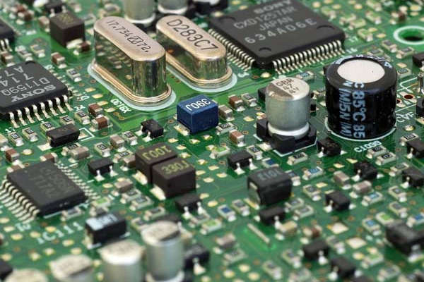
2、 Component selection principle

1. Capacitor selection
-Input filtering capacitor: Select electrolytic capacitors with low ESR (such as solid-state capacitors) and parallel high-frequency ceramic capacitors to cover wideband noise.
-Decoupling capacitors: Configure 0.1 μ F ceramic capacitors for each IC chip and add 10-100 μ F electrolytic capacitors at the power inlet. The high-frequency bypass capacitor should be close to the power supply pin and the lead should be minimized.
-Thermal circuit capacitor: Choose MLCC capacitors with excellent high-frequency characteristics and place them close to the switch tube to minimize circuit inductance.
2. Diode and rectifier
Fast recovery or Schottky diodes should be selected for the output rectifier diode to reduce the spike noise caused by reverse recovery current.
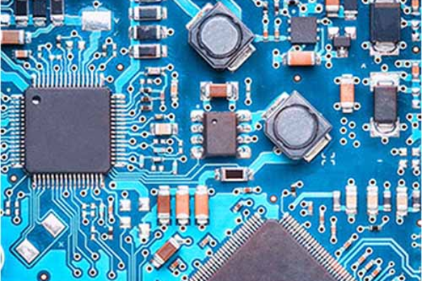
3、 PCB layout principles
1. Minimize the thermal circuit
-The high-frequency current path (such as the circuit formed by switch tubes, transformers, and capacitors) should be shortened as much as possible to reduce the equivalent series inductance (ESL) and resistance (ESR). Vertical layout decoupling capacitors (near the bottom of the switch tube) are better than horizontal layout.
-Symmetrical layout of MOSFETs and capacitors (such as 90 ° or 180 ° arrangement), and utilizing the ground layer of multilayer boards to reduce loop impedance.
2. Ground wire design
-Single point grounding combined with multi-point grounding: Low frequency circuits (<1 MHz) use single point grounding, while high-frequency circuits (>10 MHz) use multi-point grounding. Digital ground and analog ground need to be physically isolated and connected through magnetic beads or 0 Ω resistors.
-Bold ground wire: The width of the ground wire should be at least 3 mm and form a closed loop to reduce the potential difference.
3. Power and signal separation
-The layout of input/output terminals, control circuits, and power circuits should be partitioned with a minimum distance of 5 mm. High current paths (such as power lines) should be wide and short to avoid being parallel to sensitive signal lines.
-Adopting a multi-layer board design, the power layer and ground layer are separately divided to reduce radiation interference.

4. Decoupling capacitors and shielding
-The decoupling capacitor is located adjacent to the IC power pin, and the high-frequency capacitor is directly connected across the power supply and ground to avoid excessively long leads.
-For high-frequency noise sources (such as transformers), metal shielding covers should be used, and the grounding point should have low impedance. The ventilation holes should be designed as small-sized porous arrays.
4、 Testing and Validation
1. Efficiency testing
Use a power analyzer to measure input/output power, optimize switching frequency and dead time to balance efficiency and losses.

2. EMI testing
-Conducted EMI: Use LISN (Line Impedance Stabilization Network) to detect the noise spectrum at the input end and verify the performance of the filter.
-Radiated EMI: Use a spectrum analyzer to scan the 30 MHz – 1 GHz frequency band in a dark room to ensure compliance with CISPR or FCC standards.
3. Thermal performance testing
Infrared thermal imager detects hotspot distribution, optimizes heat dissipation design (such as copper foil area and heat dissipation hole layout), and ensures controllable temperature rise of power devices.
4. Simulation verification
Use tools such as Ansys Q3D and FastHenry to extract parasitic parameters, simulate ESL/ESR of thermal circuits, and optimize layout.
5、 Summary
The PCB design of efficient SMPS requires full chain coordination from circuit topology, component selection to layout optimization, with the core being to minimize parasitic parameters, optimize thermal management, and EMI suppression. By combining simulation and actual testing, iterative design can significantly improve power performance and reliability.
-600x400-c.png)