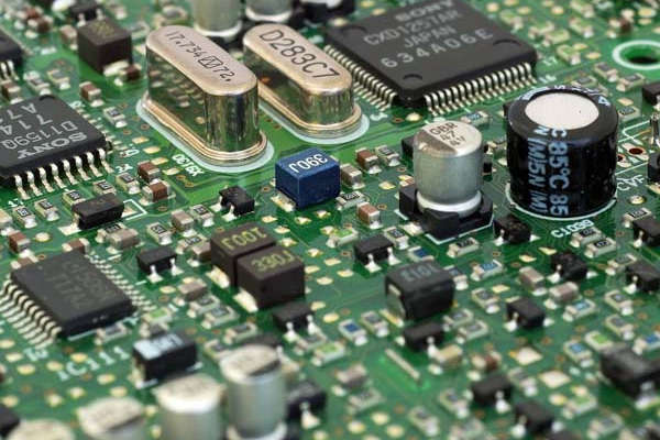
In the race for faster data transfer, your PCB isn’t just a passive carrier—it’s the active gatekeeper of USB performance. While USB standards define theoretical speeds (USB 2.0 at 480 Mbps, USB 3.0 at 5 Gbps, USB4 at 40 Gbps), real-world throughput hinges on PCB design choices that combat signal degradation, impedance mismatches, and electromagnetic interference. For engineers pushing speed limits, understanding these PCB-centric bottlenecks is critical.
Table of Contents
1. The Foundation: Differential Pairs & Impedance Control
USB 2.0: Precision at 480 Mbps
•90Ω ±10% Differential Impedance: Non-negotiable for minimizing reflections. Deviations distort eye diagrams, increase jitter, and trigger packet errors.
•Trace Geometry Rules:
–Microstrip Calculations: Impedance (Zdiff) depends on trace width (W), spacing (S), dielectric height (H), and copper thickness (T). For FR-4 (εr=4.2):
- Z<sub>o</sub> = [87/√(ε<sub>r</sub>+1.41)] × ln[5.98H/(0.8W + T)]
Z<sub>diff</sub> = 2Z<sub>o</sub>(1 – 0.48e<sup>-0.96S/H</sup>)
–Typical Values: 11-mil width + 5-mil spacing achieves 92.2Ω on 1.6-mm FR-4.
•Critical Layout Practices:
–No capacitors/ferrites on differential lines (disrupts impedance).
–Serpentine routing for length matching (max 5-mil skew).
–45° bends only—90° corners cause impedance discontinuities.
USB 3.0/3.1: Surviving the 5 Gbps Gauntlet
•Stricter Tolerance: ±5% impedance variation allowed vs. USB 2.0’s ±10%.
•Loss Budget Crisis: At 2.5 GHz Nyquist frequency:
–12-inch PCB traces consume ~3.5 dB of the 12.5 dB total loss budget.
–Solution: Low-Df Laminates (Rogers 4350B, Megtron 6) with Df ≤0.003 cut loss by 50% vs. FR-4.

2. Signal Killers: How PCB Layout Sabotages Speed
A. The Via Problem
•Stub Effects: Vias longer than 200 mils act as antennas, reflecting 28+ GHz signals in USB 3.0. Result: closed eye diagrams, failed compliance.
•Fix: Laser-drilled microvias (<0.1 mm diameter) + back-drilling for stub removal.
B. Ground Plane Fragmentation
•Split planes beneath differential pairs increase return path inductance, causing:
–EMI radiation ↑ 15 dB
–Common-mode noise triggering false symbols.
•Solution: Solid reference planes under entire USB route + guard rings with ground vias.
C. Crosstalk in High-Density Designs
•USB 3.0’s extra RX/TX pairs create cross-talk risks:
–Aggressors: DDR memory, PCIe traces
–Victim: SuperSpeed differential pairs.
•Mitigation:
–3W rule (trace spacing ≥ 3× trace width)
–Shielding cans over USB ICs.
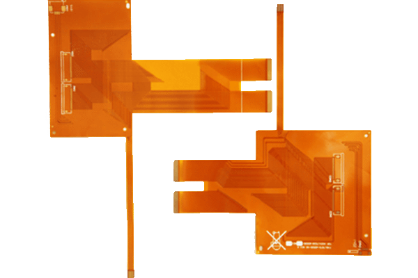
3. Connectors & Cables: The PCB’s Hidden Handoff
The Cost of Poor Connector Integration
•Case Study: Industrial cameras using L-COM cables failed at 200 MB/s due to:
–Impedance Mismatch: Connector pads deviated >20% from 90Ω spec.
–Contact Tolerance: 5° insertion angle variation caused dropouts.
•PCB Fix:
–ENIG finish for smoother pad surfaces
–Impedance-tuning near connector footprints
Cable Extension Limits
| USB Standard | Max Unassisted Length | PCB-Enabled Solution |
| USB 2.0 | 5 meters | None |
| USB 3.0 | 3 meters | Redriver ICs (e.g., PTN36241B) |
| USB4 | 0.8 meters | Retimers + low-loss flex PCBs |
4. Material Matters: When FR-4 Isn’t Enough
Performance Comparison of PCB Materials for USB 3.0+:
| Material | Df @ 10 GHz | Thermal Conductivity | Cost vs. FR-4 | Best For |
| Standard FR-4 | 0.020 | 0.3 W/(m·K) | 1.0× | USB 2.0 |
| Megtron 6 | 0.002 | 0.4 W/(m·K) | 3.2× | USB 3.0 < 2″ |
| Rogers 4350B | 0.0037 | 0.6 W/(m·K) | 6.5× | USB4, 6“+ traces |
Real-World Impact: Switching from FR-4 to Rogers 4350B for a 6-inch USB 3.0 trace:
– Insertion loss ↓ from -8.2 dB to -3.1 dB @ 5 GHz
– Achievable speed ↑ from 2.8 Gbps to 4.6 Gbps.
5. Case Study: Why “Certified” Designs Fail in Production
A power bank manufacturer faced 40% failure rates in USB-C PD boards despite passing design validation:
– Root Cause:
– 15% copper thickness variation in microvias → impedance spikes
– Inadequate thermal relief under 100W PD MOSFETs → solder reflow warpage.
– Solutions Implemented:
– Plating Uniformity Control: ≤8% thickness variation via pulse electroplating
– Embedded Copper Coins: Reduced θJA by 60% under PD controllers.
Design Rules for Maximizing USB Speeds
1.Stackup Symmetry
–Balance copper distribution layer-to-layer (<5% density variation) to prevent warpage-induced impedance shifts.
2.ESD Protection Strategy
–Place TVS diodes before series resistors—reversed order causes ESD failures.
3.Power Integrity
–Use 2-oz copper for VBUS lines + 0.1-μF/10-μF decoupling near ports.
4.3D EM Simulation
–Model insertion loss/return loss pre-layout (Keysight ADS, Ansys HFSS).
“In USB design, your PCB is the signal’s first mile and last mile—every micron of copper, every via transition, either enables speed or strangles it.”
Engineer PCBs That Deliver Promised Speeds
→ [Download Our USB Impedance Design Checklist]
→ [Request a Signal Integrity Simulation Report]
→ [Explore Our Rogers 4350B-Based Reference Designs]