Electronic Design Automation (EDA) is the $14.2 billion technological backbone enabling the creation of today’s billion-transistor chips and multilayer PCBs. For PCB manufacturers, mastering EDA workflows is no longer optional—it’s the critical bridge between circuit concepts and manufacturable designs. This guide demystifies EDA’s core mechanisms and its transformative role in electronics.
Table of Contents
1、Core Functions & Applications: From Concept to Manufacturing
1. PCB-Centric EDA Workflow

2. Key Application Scenarios
| Domain | EDA Solution | PCB Impact |
| High-Speed Design | SI/PI Analysis Tools | ±5% Impedance Control in 24L HDI |
| Power Electronics | Thermal Simulation | 40℃ Junction Temp Reduction |
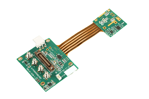
| IoT Devices | Multi-Board System Design | Rigid-Flex PCB Yield ↑30% |
| Automotive | EMI/EMC Compliance Check | Pass CISPR 25 Class 5 with Margin |
> Case Study: Nvidia’s A100 GPU PCB leveraged ANSYS HFSS to eliminate 92% of signal integrity issues pre-production.
2、Core Technologies & Tool Ecosystem
1. Foundational Technologies
– Constraint-Driven Routing
Define impedance/clearance rules (e.g., DDR4: 85Ω±5%, 3W spacing) → Auto-router generates compliant layouts
– Multi-Physics Simulation
Solve Maxwell’s equations for EMI hotspots and thermal stress points
– AI-Driven Optimization
Neural networks predict optimal component placement (e.g., reduce BGA escape routing time by 70%)
2. Industry-Standard Tool Stack
| Function | Leading Tools | PCB Advantage |
| Schematic & Layout | Altium Designer, Cadence Allegro | HDI Support: 0.1mm microvias |
| Signal Integrity | ANSYS HFSS, Keysight ADS | 112G PAM4 Eye Diagram Validation |
| DFM Analysis | Valor NPI, Siemens Ucamco | Detect 15μm copper imbalance |
| Thermal Management | COMSOL, FloTHERM | Prevent PCB delamination at 260℃ |
3、Strategic Importance & Industry Challenges
1. Why EDA is Non-Negotiable
– Complexity Management:
16-layer server PCBs contain >20,000 nets vs. 500 in 1990s designs
– Cost Prevention:
DFM checks catch 98% of fab issues pre-tapeout (vs. $500k respin cost)
– Performance Assurance:
Impedance simulation ensures <0.5dB loss at 56Gbps
2. Critical Challenges
– Tool Integration Gaps:
43% of engineers report MCAD-ECAD mismatches causing enclosure conflicts
– Skill Shortages:
ANSYS HFSS experts command $180k+ salaries amid talent scarcity
– Licensing Costs:
Full EDA suite exceeds $250k/year – prohibitive for SMEs
4、Future Trends: AI, Cloud & Quantum Leap
1. AI Revolution in EDA
– Generative Design:
Autodesk Fusion 360’s AI agent creates PCB layouts from natural language prompts (“Optimize for 10GHz RF”)
– Predictive Yield Analytics:
ML models correlate DFM violations with fab yield (98% accuracy at TSMC)
2. Cloud-Native Platforms
– Siemens Xcelerator:
Real-time collaboration for distributed teams (version conflict ↓90%)
– Cloud Compute Scaling:
8-hour EM simulation completes in 22 minutes using AWS GPU clusters
3. Emerging Frontiers
– Quantum EDA Tools:
Cadence prototyping quantum-aware routers for qubit control PCBs
– 3D IC Co-Design:
Synopsys 3D Compiler manages interposer routing in chiplet-based systems
Why This Matters to PCB Manufacturers
1. Design-Manufacturing Handoff:
ODB++/IPC-2581 intelligent data exchange eliminates Gerber misinterpretation
2. Advanced Package Support:
Embedded die PCB workflows require EDA-PLM integration
3. Sustainability Compliance:
Automated material databases track carbon footprint per IPC-1752B
→ [Download EDA-PCB Integration Checklist]
Covering tool selection criteria, DFM rule templates & cost optimization strategies