Table of Contents
Executive Summary
Co-Packaged Optics (CPO) represents a paradigm shift in data center connectivity, moving optical engines from traditional pluggable modules to direct integration with switch ASICs on a common substrate. This groundbreaking approach significantly reduces power consumption by 30-50% compared to conventional solutions while enabling unprecedented data rates of 800G, 1.6T, and beyond . For PCB manufacturers and designers, CPO introduces both challenges and opportunities—demanding advanced materials, sophisticated thermal management, and innovative layout strategies while potentially simplifying certain aspects of high-speed signal routing. As AI and machine learning workloads continue to explode, CPO technology is poised to become a critical enabler for next-generation data centers, with the global CPO market projected to reach $26 billion by 2033 .
1.Understanding CPO Technology: A Fundamental Shift
1.1 What is CPO?
Co-Packaged Optics (CPO) is an advanced packaging technology that integrates optical engines and switch chips on a common substrate or interposer, dramatically shortening the electrical connection path between compute silicon and optical components . Unlike traditional architectures where optical modules are pluggable components separated from switch ASICs, CPO brings them into intimate proximity, reducing signal path lengths from centimeters to millimeters . This fundamental architectural change addresses critical bottlenecks in modern data centers where traditional pluggable optical modules face limitations in power consumption, thermal management, and signal integrity at higher data rates.
1.2 How CPO Differs from Traditional Architectures
In conventional network switch designs, pluggable optical modules are installed on the front panel, connected to the switch ASIC through PCB traces that can be several centimeters long. These extended electrical paths result in significant signal degradation at higher data rates, requiring power-hungry retimers and complex equalization . CPO technology fundamentally rearchitects this relationship by:
•Eliminating front panel pluggable interfaces in favor of direct optical connectivity
•Reducing electrical trace lengths from centimeters to millimeters
•Integrating silicon photonics technology alongside electronic chips using advanced packaging techniques
•Moving critical interfaces from the PCB level to the package level
This architectural shift represents the most significant change in network switch design in decades, with major implications for PCB layout, material selection, and thermal management strategies.

2.Key Advantages of CPO Technology
2.1 Power Efficiency and Thermal Management
CPO’s most significant advantage is its dramatic reduction in power consumption. Research indicates that CPO technology can reduce power consumption by 30-50% compared to traditional pluggable optical modules . This exceptional efficiency stems from several factors:
•Shorter electrical paths minimize signal loss and reduce the need for power-hungry signal conditioning components
•Elimination of DSP chips in the optical path, which traditionally consume up to 50% of a module’s power
•Advanced cooling integration capabilities, including support for both air and liquid cooling systems
For large-scale data centers, these power savings translate to millions of dollars in reduced operational expenses annually and enable higher port densities without exceeding power budgets.
2.2 Enhanced Signal Integrity and Performance
By drastically shortening the electrical interface between compute silicon and optical components, CPO technology delivers superior signal integrity performance:
•Reduced signal attenuation and distortion through millimeter-scale versus centimeter-scale interconnects
•Minimized parasitic elements that degrade signal quality at high frequencies
•Support for higher data rates, with current implementations supporting 800G and 1.6T transmission, and roadmaps extending to 3.2T and beyond
These signal integrity advantages make CPO particularly valuable for AI/ML workloads that demand low-latency, high-bandwidth communication between computational elements.
2.3 System-Level Integration and Density
CPO enables unprecedented levels of integration and bandwidth density:
•Higher port densities through elimination of front-panel pluggable interfaces
•Reduced form factors, with solutions like Broadcom’s Tomahawk 5 “Bailey” integrating 51.2T of switching capacity in a palm-sized package
•Consolidated functionality through 3D chip stacking and advanced packaging technologies
This integration advantage allows data center operators to maximize computational density within fixed space and power constraints.
3.CPO vs. LPO: A Technical Comparison
3.1 Understanding LPO Technology
Linear Drive Pluggable Optics (LPO) has emerged as an alternative approach to addressing power consumption challenges in high-speed data centers. Unlike CPO, LPO maintains the familiar pluggable form factor but eliminates the power-hungry DSP chip from the module . Instead, LPO leverages high-linearity analog components—specialized driver and transimpedance amplifier (TIA) chips with integrated equalization functions—to handle signal processing tasks .
3.2 Comparative Analysis: CPO vs. LPO
Table: CPO vs. LPO Technical Comparison
| Parameter | CPO | LPO |
| Integration Level | High (optics co-packaged with ASIC) | Moderate (pluggable form factor) |
| Power Efficiency | 30-50% reduction vs. traditional | ~50% reduction in module power |
| Signal Integrity | Superior (mm-scale interconnects) | Good (dependent on PCB layout) |
| Thermal Management | Complex (requires advanced cooling) | Simplified (traditional approaches) |
| Maintenance | Challenging (component-level replacement) | Easy (hot-swappable modules) |
| Best Application | Ultra-scale AI/ML clusters | Short-reach data center links |
While LPO offers advantages in maintainability and faster time-to-market, CPO provides superior performance and efficiency for the most demanding applications . Industry analysis suggests these technologies will coexist, addressing different segments of the data center connectivity market.
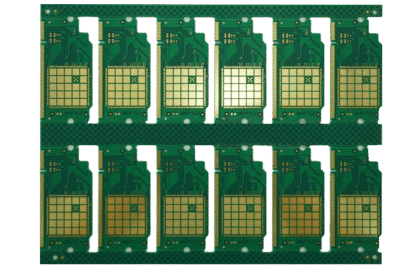
4.CPO’s Implications for PCB Design and Manufacturing
4.1 Material Selection Challenges
The implementation of CPO technology demands significant advancements in PCB materials to support its unique requirements:
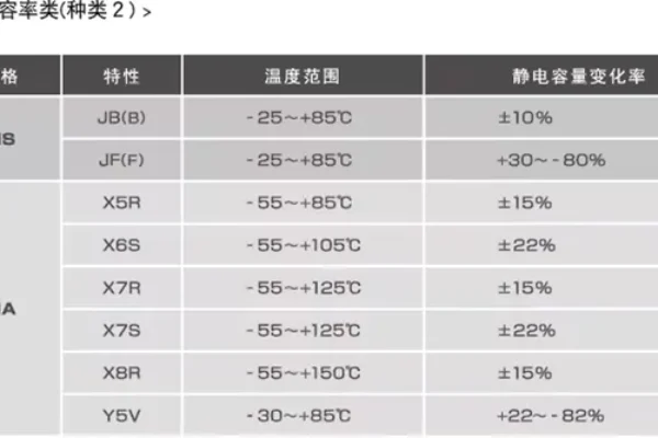
•Low-Loss Laminates: High-frequency designs require advanced substrates with controlled dielectric properties (Dk of 2.5-3.5 with tight tolerance) and low loss tangents (<0.001-0.002) to minimize signal loss
•Enhanced Thermal Management: PCB materials with higher thermal conductivity (≥0.5 W/m/K) are essential to handle concentrated heat from co-packaged modules
•Dimensional Stability: Materials with high stability across temperature ranges are critical for impedance control in CPO-adjacent circuits
These material requirements represent a significant shift from conventional PCB substrates and necessitate closer collaboration between PCB manufacturers and material suppliers.
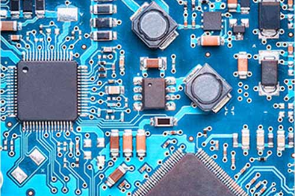
4.2 Layout and Routing Considerations
CPO technology fundamentally changes PCB layout priorities and constraints:
•Reduced High-Speed Routing: With critical interfaces moving to the package level, the PCB primarily serves power delivery and low-speed control functions
•Power Integrity Challenges: Sophisticated power delivery networks with multiple power planes and strategic decoupling capacitor placement are essential for clean power to CPO modules
•Thermal Relief Patterns: Advanced thermal via patterns and heat spreaders are necessary to manage localized hot spots
These changes require PCB designers to develop new skill sets and design methodologies tailored to CPO systems.
4.3 Thermal Management Strategies
Effective thermal management is arguably the most critical challenge in CPO system design:
•Advanced Cooling Solutions: CPO systems often require sophisticated approaches such as microchannels for liquid cooling or advanced thermal interface materials
•Thermal Via Patterns: Strategic placement of thermal vias under power components helps dissipate heat from co-packaged optics
•Copper Thickness Optimization: Appropriate copper weights ensure adequate current carrying capacity and heat spreading
PCB designers must work closely with mechanical and thermal engineers to develop holistic cooling solutions for CPO systems.

5.Current State of CPO Development and Deployment
5.1 Industry Leader Initiatives
Major technology companies are driving CPO development and commercialization:
•Broadcom: Their Tomahawk series switches, including the Tomahawk 5 “Bailey” (8×6.4T optical engines) and upcoming 3nm Tomahawk 6 (102.4T), represent some of the most advanced CPO implementations
•NVIDIA: Quantum-X800 CPO switches are scheduled for deployment in 2025-2026, with future architectures like “Feynman” incorporating 204T CPO switches
•Ayar Labs & Alchip: Their collaboration focuses on CPO solutions featuring over 100Tbps of scale-up bandwidth per accelerator and support for more than 256 optical scale-up ports per device
These developments indicate strong momentum behind CPO technology despite the technical challenges.
5.2 Commercial Timeline and Market Projections
CPO technology is transitioning from research to commercial deployment:
•2024-2025: Initial commercial deployments begin with 800G and 1.6T ports
•2026-2027: Period of scaled growth expected as manufacturing matures and costs decline
•2033: Global CPO market projected to reach $26 billion
Industry leaders like Broadcom are already shipping initial CPO systems to select customers, with broader availability expected in the 2025-2026 timeframe .
6.Challenges and Limitations of CPO Technology
6.1 Technical Hurdles
Despite its promise, CPO faces significant technical challenges:
•Thermal Management: Concentrating both optical and electronic functions creates significant thermal density that requires advanced cooling solutions
•Manufacturing Complexity: CPO requires sophisticated packaging technologies such as silicon interposers with through-silicon vias (TSVs), leading to yield challenges
•Reliability Concerns: Integrating multiple optical modules with chips increases failure rates, with some implementations showing order-of-magnitude increases in failure probability
6.2 Economic and Ecosystem Challenges
Beyond technical issues, CPO faces business and ecosystem challenges:
•High Initial Costs: Current CPO implementations carry significant cost premiums, with 1.6T CPO ports costing approximately 2.3x more than pluggable alternatives
•Maintenance Complexity: Non-pluggable architecture complicates repairs, with some estimates suggesting 6x longer repair times compared to pluggable modules
•Standardization Gaps: Multiple competing standards (COBO, OIF, OpenEye) create compatibility challenges and increase development costs
These challenges have led some cloud service providers to approach CPO cautiously, potentially slowing widespread adoption .
7.The Future of CPO in Data Center Infrastructure
7.1 Technology Roadmaps
Leading companies have articulated clear CPO development trajectories:
•Speed Evolution: Progression from current 51.2T implementations to 102.4T (Tomahawk 6) and 204T (NVIDIA Feynman) platforms
•Process Advancement: Migration to more advanced nodes, such as Broadcom’s Tomahawk 6 utilizing TSMC’s 3nm process
•Packaging Innovation: Development of more integrated approaches like TSMC’s COUPE (Compact Universal Photonic Engine) platform
These roadmaps suggest steady progress in CPO capabilities through the end of the decade.
7.2 Long-Term Outlook
While challenges remain, the long-term outlook for CPO appears strong:
•AI/ML Driving Adoption: Explosive growth in AI workloads will create strong demand for CPO’s high-bandwidth, low-power characteristics
•Hybrid Approaches: Coexistence with refined pluggable optics (including LPO) for different application segments
•Ecosystem Development: Maturing of design tools, testing methodologies, and industry standards to support broader adoption
For PCB manufacturers, CPO represents both a disruptive threat to traditional high-speed board design and an opportunity to provide more value through advanced materials and design expertise.
8.Conclusion
CPO technology represents a fundamental architectural shift in data center connectivity, offering compelling advantages in power efficiency, signal integrity, and integration density. While technical and economic challenges remain, the strong industry commitment from leaders like Broadcom, NVIDIA, and TSMC suggests CPO will play an increasingly important role in future AI/ML infrastructure.
For PCB manufacturers and designers, CPO demands new capabilities in advanced materials, thermal management, and system-level design while potentially simplifying certain aspects of high-speed layout. Companies that develop expertise in CPO-adjacent technologies—including low-loss materials, sophisticated power delivery, and advanced thermal management—will be well-positioned to support this emerging paradigm.
As data centers continue to evolve to support increasingly demanding AI workloads, CPO technology offers a path to the higher efficiencies and densities required for next-generation computational infrastructure. The coming years will be critical in determining CPO’s ultimate position in the connectivity landscape, but its potential to transform data center economics and capabilities is undeniable.
Partner with Us for Your Advanced PCB Requirements
As CPO technology continues to evolve, the demands on PCB design and manufacturing will intensify. Our expertise in advanced PCB fabrication positions us uniquely to support the development of cutting-edge CPO infrastructure. From low-loss materials to sophisticated thermal management solutions, we provide the technological foundation for tomorrow’s AI breakthroughs.
Contact us today to discuss how our PCB capabilities can support your CPO technology requirements and help build the infrastructure needed for the next generation of artificial intelligence evolution.