Table of Contents
Executive Summary
PCB stamp holes, also known as breakaway holes or mouse bites, are a crucial technology in printed circuit board manufacturing and assembly. These small, strategically placed holes along PCB edges enable efficient panelization and separation of circuit boards while providing mechanical stability during the manufacturing process. This comprehensive guide explores stamp hole design principles, applications, advantages, limitations, and best practices to help electronics manufacturers optimize their PCB designs for manufacturability and reliability. Understanding proper stamp hole implementation is essential for reducing production costs, improving assembly efficiency, and ensuring final product quality in modern electronic devices.
1.Introduction to PCB Stamp Holes
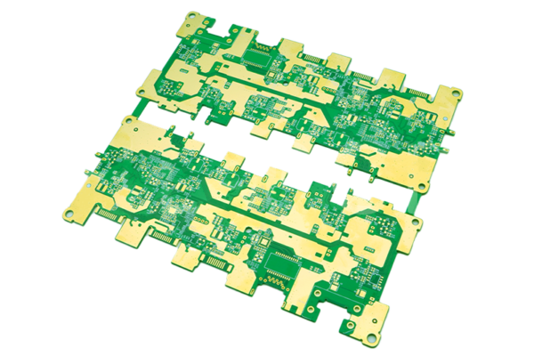
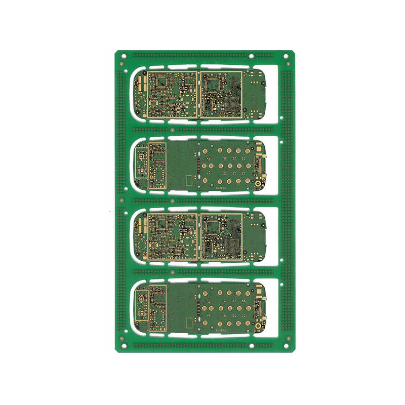
PCB stamp holes are small, evenly spaced holes drilled along the borders between individual circuit boards in a panelized array. Named for their resemblance to the perforations between postage stamps, these features create weakened lines that allow clean separation of individual boards after assembly .
The practice of panelization involves arranging multiple PCBs onto a single panel for manufacturing efficiency, and stamp holes serve as one of the primary methods for connecting these individual boards within the panel . Unlike V-scoring which creates V-shaped grooves along straight lines, stamp holes can accommodate complex board geometries including curves, angles, and irregular shapes . This flexibility makes stamp holes particularly valuable for prototyping and manufacturing PCBs with non-rectangular outlines.
Stamp holes function by creating a perforated separation line that maintains sufficient mechanical strength to survive the rigors of automated assembly while allowing relatively easy separation once component installation is complete. The technology represents a balance between connection integrity and separation convenience in PCB manufacturing.

2.Stamp Hole Design Specifications and Parameters
Proper stamp hole design requires careful attention to dimensional parameters to ensure optimal mechanical strength and separation characteristics.
2.1 Standard Dimensions and Configurations
Well-designed stamp holes follow established industry specifications that balance connection strength with clean separability:
•Hole diameter: Typically 0.6mm is recommended, though diameters may range from 0.6mm to 1.2mm depending on board thickness and application requirements .
•Number of holes: Generally 5-8 holes per connection point are recommended, with a minimum of 5 holes to ensure adequate strength . Each connection point should contain sufficient holes to distribute mechanical stress during handling and assembly.
•Hole spacing: The distance between hole centers is typically 1.0mm, with edge-to-edge spacing of approximately 0.2-0.4mm . This spacing creates the characteristic perforated appearance while maintaining structural integrity.
•Panel spacing: Boards connected via stamp holes typically maintain 1.6mm to 2.0mm between adjacent board edges, with a minimum spacing of 1.2mm to facilitate clean separation .
2.2 Optimal Placement Strategies
Strategic placement of stamp holes significantly impacts both manufacturability and final board quality:
•Board integration: Stamp holes should be positioned along the centerline of the board edge or extended slightly into the board (approximately 1/3 of the hole diameter) to minimize protrusions after separation .
•Clearance from components: Stamp holes must maintain adequate distance from nearby traces, components, and vias to prevent damage during separation .
•Connection points: The number of stamp hole connection points should be proportional to board size, with additional connections added approximately every 50-60mm for larger boards .
•Stress distribution: Stamp holes should be concentrated in areas with minimal stress concentration during normal board operation, avoiding locations subject to mechanical flexing or thermal expansion.
3.Applications and Use Cases
Stamp hole technology serves multiple critical functions in PCB manufacturing and electronic product development:
3.1 PCB Panelization
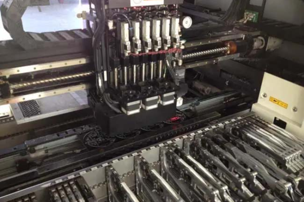
The primary application of stamp holes is in PCB panelization, where multiple individual boards are manufactured as a single composite panel for processing efficiency . This approach significantly enhances production efficiency for automated assembly equipment, particularly for smaller boards that would be difficult to handle individually. The stamp holes provide sufficient mechanical strength to withstand the SMT process while allowing straightforward separation afterward.
3.2 Irregular Board Shapes
Unlike V-scoring which is limited to straight-line separations, stamp holes can accommodate complex board geometries including circular, curved, or highly irregular outlines . This capability makes stamp holes particularly valuable for manufacturing non-rectangular PCBs commonly found in consumer electronics, wearable devices, and specialized industrial equipment where form factor constraints dictate unconventional board shapes.
3.3 Module Integration
Stamp holes enable the creation of modular circuit boards that can be mounted directly onto larger parent PCBs . This approach is commonly used for system-on-module designs, wireless communication modules (Wi-Fi, Bluetooth), and other functional blocks that benefit from pre-assembled testing before integration into final products. The stamp holes in these applications often serve both mechanical connection and electrical connection purposes.
3.4 Thin PCB Applications
For circuit boards with thickness below 1.2mm, V-scoring becomes problematic due to insufficient material for proper groove formation . Stamp holes provide a reliable alternative for panelizing thin PCBs where V-scoring would compromise structural integrity or create manufacturing difficulties.
4.Advantages and Limitations
Understanding the trade-offs of stamp hole technology is essential for appropriate implementation:
4.1 Key Advantages
•Geometric flexibility: Unlike V-scoring, stamp holes support virtually any separation contour including curves, angles, and complex shapes .
•Equipment accessibility: Separation typically requires only simple tools, making stamp holes accessible for low-volume production and prototyping scenarios where dedicated separation equipment is unavailable .
•Suitability for thin boards: Stamp holes work effectively with thin PCB materials that are problematic for V-scoring .
•Module integration: The technology enables direct soldering of daughter boards to parent PCBs, eliminating connectors and reducing profile height in stacked configurations .
•Prototyping efficiency: During development phases, stamp holes allow manufacturers to produce multiple design variations in a single panel, streamlining the prototyping process.
4.2 Limitations and Challenges
•Edge quality: Separation typically leaves irregular protrusions resembling saw teeth (often called “dog teeth”) along the board edge, which may require secondary operations for applications where clean edges are critical .
•Stress concentration: The perforated nature of stamp hole connections can create localized stress points during separation, potentially damaging delicate components if not properly designed .
•Labor requirements: Manual separation of stamp hole panels can be labor-intensive compared to V-scoring, particularly for high-volume production .
•Board space utilization: The additional space required for stamp hole connections slightly reduces panel utilization efficiency compared to V-scoring .
•Process inconsistency: Manual separation may introduce variability in edge quality compared to machine-controlled V-scoring separation .
5.Stamp Holes vs. V-Scoring: A Comparative Analysis
Selecting between stamp holes and V-scoring requires understanding their respective characteristics:
Table: Comparison between Stamp Holes and V-Scoring Techniques
| Parameter | Stamp Holes | V-Scoring |
| Board Geometry | Supports complex shapes, curves, and irregular outlines | Limited to straight-line separations |
| Edge Quality | Irregular protrusions typically require secondary finishing | Clean, straight edges with minimal post-processing |
| Suitable Board Thickness | Effective for thin boards (<1.2mm) | Problematic for very thin substrates |
| Tooling Requirements | Basic tools sufficient for separation | Specialized V-scoring equipment required |
| Typical Applications | Irregular boards, module-on-module, thin PCBs | Rectangular boards, high-volume production |
| Panel Strength | Moderate, with potential stress concentration at holes | Generally robust along the V-groove line |
6.Manufacturing Process and Quality Control
The production of PCBs with stamp holes follows a specialized process sequence:
6.1 Fabrication Workflow
•Drilling phase: Stamp holes are typically drilled during the same operation as other PCB vias and through-holes, ensuring positional accuracy relative to other board features .
•Plating process: Like other holes in the PCB, stamp holes generally receive electroless copper plating to create conductive pathways if needed for electrical connectivity .
•Panel separation: After component assembly, boards are separated by applying controlled force to break the material bridges between stamp holes . This can be performed manually for prototypes or low volumes, or using specialized equipment for production quantities.
6.2 Quality Assurance Measures
•Dimensional verification: Stamp hole diameter, position, and spacing should be verified against design specifications .
•Visual inspection: Plating quality and hole integrity should be checked before panelization .
•Separation testing: Sample panels should be separated and examined for edge quality and any evidence of delamination or cracking .
•Deburring operations: For applications requiring smooth edges, mechanical deburring or sanding may be necessary after separation .
7.Best Practices for Optimal Stamp Hole Implementation
Maximizing the benefits of stamp hole technology requires adherence to established design and manufacturing guidelines:
7.1 Design for Manufacturability (DFM)
•Hole placement: Position stamp holes to avoid extending beyond the board edge after separation by centering them on the board outline or slightly inward .
•Copper clearance: Maintain adequate distance between stamp holes and nearby circuits to prevent damage during separation .
•Support requirements: Include sufficient stamp hole connections to prevent panel flexure during assembly, typically adding extra connections for larger boards or those with heavy components .
•Material considerations: Account for PCB substrate characteristics, as different materials exhibit varying separation behaviors .
7.2 Design for Assembly (DFA)
•Panel strength: Ensure stamp hole connections provide adequate strength to survive SMT processes including solder paste printing, component placement, and reflow soldering .
•Fixture requirements: For automated assembly, design panels with sufficient rigidity to prevent flexing during handling, potentially incorporating additional support structures .
•Separation access: Allow adequate clearance around separation lines for tools or fixtures in high-volume production environments.
7.3 Advanced Design Techniques
•Improved designs: More advanced stamp hole configurations position the edge of the material bridges at the centerline of the outermost holes, creating cleaner breaks with less protruding material .
•Selective strengthening: In panels with varying support needs, increase stamp hole density in areas subject to greater stress while maintaining standard spacing in other regions.
•Mixed separation methods: Combine stamp holes with limited V-scoring in panel designs that include both regular and irregular board outlines.
8.Future Trends and Developments
Stamp hole technology continues to evolve in response to changing industry requirements:
•Miniaturization: As electronic devices shrink, stamp hole dimensions are decreasing accordingly, with finer pitches and smaller diameters becoming more common .
•Automated separation: Improved mechanical separation equipment is being developed to handle stamp hole panels with greater consistency and reduced labor .
•Material advancements: New PCB substrate materials with enhanced mechanical properties may improve separation quality and edge characteristics .
•Design integration: PCB design software is incorporating more sophisticated stamp hole design tools with automated optimization features .
9.Conclusion
PCB stamp holes represent a versatile and essential technology in modern circuit board manufacturing, particularly valuable for irregular board geometries, module integration, and thin PCB applications. While presenting certain challenges in edge quality and separation consistency, their flexibility and accessibility make them indispensable for numerous electronic manufacturing scenarios.
By adhering to established design guidelines—including proper hole sizing (typically 0.6mm diameter), appropriate spacing (1.0mm center-to-center), and strategic placement (centered on board edges)—manufacturers can leverage stamp holes to enhance production efficiency while maintaining product quality. As electronic devices continue to evolve toward more compact and specialized form factors, stamp hole technology will remain a critical enabler for innovative PCB designs and manufacturing approaches.
Partner with Us for Your PCB Manufacturing Needs
Our expertise in advanced PCB manufacturing and precision stamp hole technology ensures that your designs are translated into reliable, high-quality circuit boards. We combine rigorous quality control with extensive manufacturing experience to deliver optimal solutions for both conventional and challenging PCB configurations.
Contact us today to discuss how we can support your specific PCB requirements with robust stamp hole implementations and comprehensive manufacturing capabilities.