In today’s rapidly iterating electronic products, PCB, as the “nerve center” of electronic devices, continues to increase in manufacturing process complexity. Especially in high-end fields such as high multi-layer boards and high-frequency high-speed boards, pcb board manufacturing need to overcome the following five core difficulties in order to ensure product reliability and market competitiveness.
Table of Contents
1、 pcb board manufacturing:Inter layer alignment deviation: a technical barrier for precision stacking
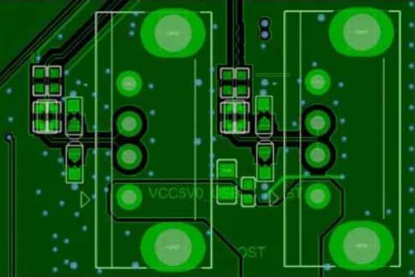
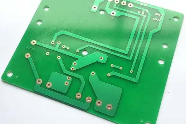
PCBs with 8 or more layers need to undergo multiple lamination processes, and interlayer offset can easily lead to short circuits or open circuits. Traditional equipment errors (± 50 μ m) are difficult to meet high-density interconnect requirements. Solution:
-Laser positioning+AOI optical alignment system: compresses errors to within ± 25 μ m, combined with real-time X-ray calibration to ensure accurate interlayer positioning;
-Application of high TG materials: Using sheet materials with Tg ≥ 170 ℃ to reduce hot pressing deformation, combined with four slot positioning (Pin LAM) and hot melt rivets to optimize stacking stability.

2、 Impedance control misalignment: the lifeline of high-speed signal transmission
High frequency signals have strict requirements for impedance tolerance (± 10%), and uneven media or excessive etching can cause signal attenuation. Innovation strategy:
-Simulation pre calculation: With the help of software such as Polar SI9000, accurately design line width/spacing, and eliminate Stub effect through back drilling technology;
-High frequency board selection: Rogers or Isola low dielectric constant (Dk) materials are used to strictly control the fluctuation of dielectric thickness.
3、 Uneven heat dissipation and thermal stress challenges

The power devices in multi-layer boards are densely packed, and thermal stress concentration can easily lead to delamination or solder joint failure. Response plan:
-Embedded heat dissipation design: copper coins are embedded to enhance local heat dissipation, combined with 2oz thick copper wiring to improve thermal conductivity efficiency;
-Hole filling electroplating process: Applying pulse electroplating technology in blind buried hole structures to enhance vertical thermal conductivity.
4、 The bottleneck of micro hole processing and drilling accuracy
The high-density interconnect (HDI) board requires a pore size of<0.1mm, and the roughness of the pore wall affects the uniformity of copper plating. Technological breakthrough:
-Composite laser drilling: using UV+CO ₂ laser combination to reduce the roughness of the hole wall to Ra<0.8 μ m, avoiding residue of adhesive residue;
-Optimization of anti breakage knife: For thick copper plates and high Tg materials, optimize drilling parameters to ensure hole spacing ≥ 0.3mm and reduce the risk of CAF effect.
5、 Whole process quality control and digital upgrade
From design to mass production, it requires crossing 22+quality inspection nodes, and traditional manual inspection is difficult to ensure consistency. Digital empowerment:
-Intelligent Manufacturing System: Deploying MES, QMS and other systems to achieve real-time monitoring of production data and 4M traceability, with a yield rate increased to over 98%;
-AI warning mechanism: Automatically collect detection data through the QCData platform, provide real-time alerts for anomalies, and shorten the response cycle for quality issues by up to 40%.
Conclusion
Faced with the multidimensional challenges of pcb board manufacturing, enterprises need to build a full chain solution covering design, production, and testing with material innovation, process upgrading, and intelligent control as the core. By introducing high-precision equipment (such as laser drills, LDI exposure machines) and digital management systems, product yield and delivery efficiency can be significantly improved, empowering customers to continue leading in fields such as 5G, AI, and automotive electronics.
Contact us immediately to obtain the “8-Layer PCB Design Guide” and customized manufacturing solutions to help your project efficiently land!