In electronic product development, PCB board design is a key bridge connecting principles and physical objects. As a professional PCB enterprise, we have summarized the following standardized design processes to help customers shorten their research and development cycles and improve product reliability.
Table of Contents
1、 Pre preparation: Accurately build the design foundation
1. Component library and schematic construction
-Create a PCB packaging library (such as SMD, BGA, etc.) according to the device specification book, prioritizing ensuring that the pad size is 0.2-0.4mm larger than the pin size to be compatible with the soldering process.
-Synchronize the establishment of a schematic symbol library to ensure that pin attributes correspond one-to-one with PCB packaging, avoiding connection errors caused by hidden pins.

2. EDA tool selection
-We recommend using Altium Designer or Jialichuang EDA (a free domestic tool). The former is suitable for complex multi-layer board design, while the latter supports rapid prototyping and supply chain integration.
2、 Structural planning: Balancing functionality and manufacturability
1. Mechanical positioning and stacking design

-According to the equipment space definition board size, place positioning components such as connectors and screw holes, and clarify the wiring exclusion zone (such as the non wiring zone around screw holes ≥ 0.5mm).
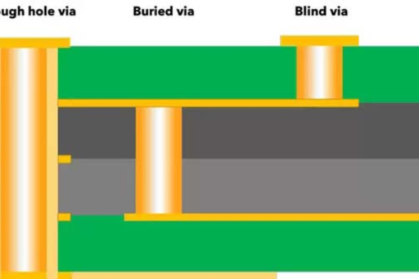
-The multi-layer board adopts a stacked structure of “signal layer ground plane power layer”, and the 6-layer board can increase the signal layer to improve the wiring density.
3、 Layout optimization: Balancing electrical performance and heat dissipation requirements
1. Functional zoning principle
-Independent layout of digital circuits, analog circuits, and power drive areas to avoid signal interference.
-The clock device is located near the load IC, and the heating element (such as power MOS transistor) is far away from the temperature sensitive device and equipped with a heat dissipation channel.
2. Decoupling capacitor arrangement
-Place a 0.1 μ F high-frequency monolithic capacitor near each IC power pin, and add a tantalum capacitor at the power inlet to ensure stable power supply.
4、 Efficient cabling: the core guarantee of signal integrity
1. Priority strategy
-First, install the power supply and ground wire (recommended width: ground wire>2.5mm, power wire>1.2mm), and then process the high-frequency signal and clock wire.
-Using 45 ° polylines or arcs to reduce radiation, high-speed differential lines are strictly of equal length and spaced at intervals of ≥ 3W (3 times the line width).

2. Via and impedance control
-The diameter of the through-hole should be ≥ 1/10 of the plate thickness (for example, a 1.6mm plate thickness requires a hole diameter ≥ 0.16mm), and when changing layers for high-frequency signals, additional through holes should be added to maintain the continuity of the reference plane.
5、 Verification and output: strict control of design quality
1. DRC and signal integrity check
-Use network inspection tools to compare the schematic and PCB connection relationship, and verify process constraints such as line spacing and aperture through Design Rule Check (DRC).
2. Copper laying and silk screen optimization
-When laying on a large area, grid copper (line width 0.3mm/spacing 0.5mm) is used, and silk screen text avoids solder pads and mirrors the bottom layer markings.
6、 Technological innovation: AI empowers efficient design
Introduce tools such as Cadence Allegro X AI to automatically complete device layout and critical wiring through generative AI, compressing traditional days’ tasks to minutes while optimizing signal integrity.
Conclusion: Professional design drives product competitiveness
Following standardized processes and combining them with intelligent tools can significantly improve PCB board design efficiency and yield. As your partner, we provide one-stop services from EDA support to fast prototyping to help you seize market opportunities.
Consult now to obtain the “Multilayer PCB board design Specification Manual” and free DFM analysis!