SysPCB is a leading PCB and SMT manufacturer in China. The following is a detailed comparison of the advantages, disadvantages, and application areas of DIP (Dual In Line Packaging) and SMT (Surface Mount Technology) in the field of electronic packaging:
Table of Contents
Advantages, disadvantages, and application areas of DIP
Advantage
- Simple structure and high reliability
-The pins are thick and sturdy, with high mechanical strength and resistance to insertion and manual soldering, making them suitable for prototype development or small-scale production.
-The welding points are visible for easy inspection and maintenance. - Strong compatibility
-Suitable for traditional through hole PCB design, with good compatibility with older equipment and experimental boards. - Good heat dissipation performance
-The package has a large volume and sufficient heat dissipation area, making it suitable for low to medium power devices. - Low cost (small batch scenarios)
-No high-precision equipment is required, manual welding or simple wave soldering can be completed.

Disadvantage
- Large volume, low density
-The wide pin spacing (such as 2.54mm) occupies a large PCB area and cannot meet modern miniaturization requirements. - Low efficiency of automated production
-Perforation design is required, making it difficult to achieve fully automated mounting and high production costs for large-scale production. - High frequency performance is limited
-The pins are long and the parasitic inductance/capacitance is large, which affects the transmission of high-frequency signals and is not suitable for high-speed circuits.
Application Fields
-Educational/Experimental Scenarios
Electronic teaching kits, breadboard experiments (such as Arduino development boards).
-Traditional industrial equipment
old controllers, power modules, relays, and other areas that are not sensitive to volume.
-Discrete component packaging
Some power devices (such as TO-220 packaged transistors) still use a DIP like structure.
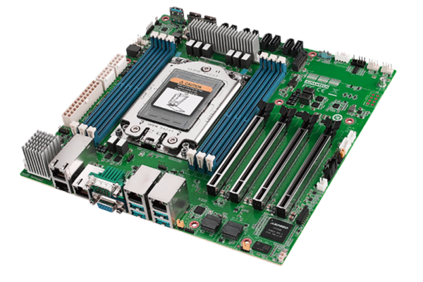
Advantages, disadvantages, and application areas of SMT
Advantage
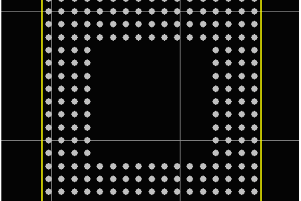
- High density and miniaturization
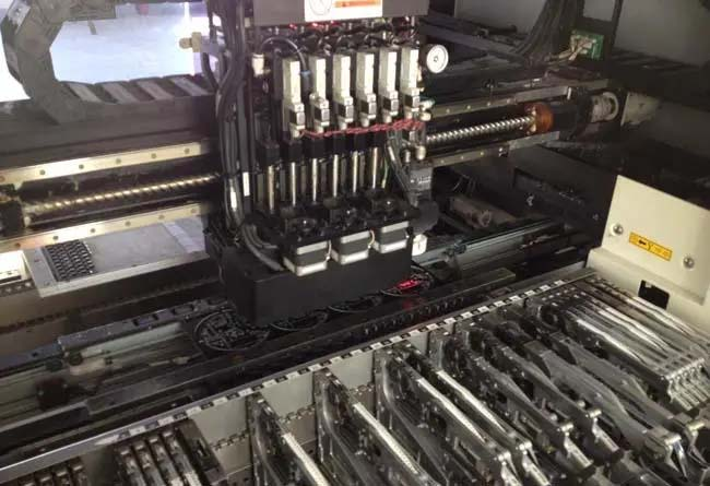
-The components are directly mounted on the surface of the PCB, with small pin spacing (such as 0.5mm), supporting multi-layer wiring, and the circuit board volume can be reduced by more than 60%. - Automation and high efficiency
-The fully automatic surface mount machine achieves high-speed production (tens of thousands of points per hour), suitable for large-scale manufacturing, and has lower overall costs. - Excellent high-frequency performance
-Short pins with minimal parasitic effects, suitable for high-speed digital circuits such as CPUs and RF modules. - Lightweight and Thinning
-No perforation design, thinner PCB thickness, meeting the lightweight needs of mobile phones, wearable devices, and more.
Disadvantage
High maintenance difficulty
-The component size is small (such as 0402 packaging), requiring a dedicated repair station and microscope operation, and manual repair is almost impossible.
Large initial investment
-Surface mount machines, reflow soldering furnaces, and other equipment are expensive, and small-scale production has poor economic efficiency.
Thermal stress sensitivity
-The welding process requires high-temperature reflow, which requires high heat resistance of the components, and may cause cracking of the solder joints due to mismatched thermal expansion coefficients.
Application Fields
–Consumer electronics: ultra-thin devices such as smartphones, laptops, TWS earphones, etc.
-High frequency/high-speed circuits: 5G communication modules, Wi Fi chips, GPU/FPGA and other integrated circuits.
–Automotive electronics: ECU control unit, ADAS sensors, meeting high reliability and vibration resistance requirements.
-Aerospace: Scenarios such as satellites and radar systems that require strict requirements for lightweight and performance.
| Features | DIP | SMT |
| Density | Low (large pin spacing) | High (small pin spacing) |
| Production mode | Manual/Semi automatic | Fully automatic |
| Cost | Low for small batches, high for large batches | High for small batches, low for large batches |
| Repair difficulty | Easy (direct welding replacement) | Difficult (requires professional equipment) |
| Applicable scenarios | Prototype validation, traditional devices | Modern electronics, miniaturized devices |
Summarize
-DIP is a “classic solution” in the field of electronic packaging, with the advantages of ease of use and reliability, but it has gradually been replaced by SMT and only exists in specific scenarios.
-SMT is currently the mainstream electronic manufacturing technology, which excels in high density and automation, but requires high-precision equipment and process control.
In practical applications, hybrid technology (DIP+SMT) is also common. For example, in industrial control boards, power devices are packaged in DIP, while digital chips are packaged in SMT to balance heat dissipation and integration requirements.