There are various types packaging method of IC, and different packaging technologies are suitable for different application scenarios, each with its own advantages and disadvantages. The following comprehensive search results list common encapsulation methods and their characteristics:
Table of Contents
1. Dual in-line package (DIP)
-Definition: The pins are arranged in a double row and need to be inserted into circuit board solder holes for soldering.
-Advantages:
-Simple structure, low cost, suitable for laboratory debugging and manual welding.
-High reliability, suitable for small and medium-sized integrated circuits (such as logic ICs and memory).
-Disadvantages:
-Large size, limited pin count (usually not exceeding 100), unable to meet high-density integration requirements.
-Poor high-frequency performance and weak anti-interference ability.
-Application scenarios: early household appliances, calculators, simple control circuits, etc.

2. Quad Flat Package (QFP/PFP)
-Definition: Surface mount packaging, with pins extending from four sides in a flat arrangement.

-Advantages:
-High pin density (up to hundreds), suitable for high-frequency applications.
-Smaller in size, with better anti-interference performance than DIP.
-Disadvantages:
-The pins are prone to bending and deformation, making it difficult to inspect after welding.
-The heat dissipation performance is average and not suitable for high-power scenarios.
-Application scenarios: Microcontrollers (MCUs), communication ICs, and low to medium power integrated circuits.
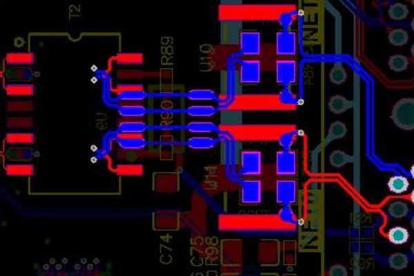
3. Ball Grid Array Packaging (BGA)
-Definition: Use a solder ball array at the bottom instead of pins, and connect the circuit board through reflow soldering.
-Advantages:
-The pin density is extremely high (up to thousands), and the signal transmission path is short, making it suitable for high-speed signals.
-Excellent heat dissipation performance and high mechanical strength (good seismic resistance).
-Disadvantages:
-Difficult to detect and repair after welding, requiring reliance on X-ray testing equipment.
-The packaging cost is high, and strict requirements are placed on PCB design.
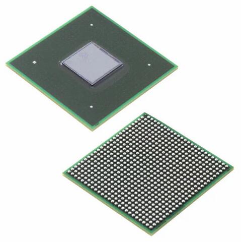
-Application scenarios: CPU、GPU、 High end processors and high-density storage ICs.
4. Pin free Quad Flat Package (QFN)
-Definition: Pin free design, with solder pads and heat dissipation pads at the bottom.

-Advantages:
-Small size, thin thickness (<1mm), suitable for portable devices.
-Good heat dissipation performance (large bottom heat dissipation pads), stable electrical performance.
-Disadvantages:
-Welding alignment is difficult and repair is challenging.
-The number of pins is limited and the scalability is weak.
-Application scenarios: Mobile device power management IC, RF module, sensors.
Development Trends of Packaging Technology
1. The rise of advanced packaging: technologies such as fan out packaging (FOWLP) and 3D stacked packaging have become mainstream to meet high computing power demands.
2. Testing technology upgrade: X-ray non-destructive testing and AOI (automatic optical inspection) are used for quality control of high-density packaging.
3. Industry chain integration: Wafer fabs and packaging and testing factories collaborate to develop intermediate processes (such as TSV through silicon vias and RDL rewiring), promoting the formation of a virtual IDM ecosystem.
Summarize
The selection of different packaging methods for ICs needs to weigh factors such as performance, volume, cost, and heat dissipation. Traditional packaging (such as DIP, QFP) is still widely used in the mid to low end market, while BGA, CSP, and advanced packaging (such as SiP, Chiplet) dominate the high-performance field. In the future, with the advancement of technologies such as AI and 5G, the packaging method of IC will further develop towards high-density and heterogeneous integration.