In the design and production of PCB (printed circuit board), positioning holes are a type of mechanical holes specially reserved for precise positioning or fixation. Their core function is to ensure the accurate and stable position of PCB in various stages (production, assembly, testing, etc.) through cooperation with external fixtures, equipment or structures.
Table of Contents
Ⅰ.Definition of positioning hole
Positioning holes are non-conductive mechanical holes on PCBs (different from vias used for conductivity), usually pre planned in position and size during design, and synchronously machined (drilled or milled) during the manufacturing stage. Its function does not involve electrical connections and is only used for mechanical positioning or fixation. It is a key design to ensure the accuracy of PCB production and the reliability of subsequent processes.
Ⅱ. The main types of positioning holes
The classification of positioning holes can be based on their functions, accuracy requirements, or application scenarios. The common types are as follows:
1. Classify by functional scenario
-Production positioning hole: used for positioning in the PCB manufacturing process, such as inner layer board pressing, exposure, etching, drilling and other processes.
For example, when laminating multi-layer boards, it is necessary to ensure precise alignment of each layer’s graphics through positioning holes (to avoid short circuits/open circuits caused by interlayer misalignment); In the exposure process, positioning holes are used to align the PCB with the mask (film) to ensure the accuracy of circuit pattern transfer.

-Assembly positioning hole: used for positioning during PCB assembly stage, the core is to ensure the accuracy of component mounting or plug-in.
For example, in SMT (Surface Mount Technology), the placement machine determines the coordinate origin of the PCB by identifying the positioning holes, ensuring accurate placement of resistors, chips, and other components onto the solder pads; When manually inserting, the positioning holes can be used to fix the PCB with fixtures to prevent displacement during assembly.
-Test positioning hole: used for positioning in the PCB testing process to ensure accurate docking between the testing fixture and the testing points on the PCB.
For example, in ICT (online testing) or FCT (functional testing), the probe of the testing fixture needs to be positioned through the positioning hole to accurately contact the testing point on the PCB, avoiding false or missed testing.
2. Classify according to accuracy requirements
-Precision positioning hole: It needs to meet high-precision tolerances (such as diameter tolerance ± 0.02mm, position tolerance ± 0.05mm), and is used in scenarios that require extremely high positioning accuracy (such as SMT mounting, multi-layer board pressing).
If the accuracy is insufficient, it may lead to misalignment (misalignment of component solder pads) or interlayer short circuits, directly affecting product yield.
-Ordinary positioning hole: with low precision requirements (such as diameter tolerance ± 0.1mm), used in scenarios where positioning accuracy is not high (such as manual assembly, simple fixation).
3. Classify by location
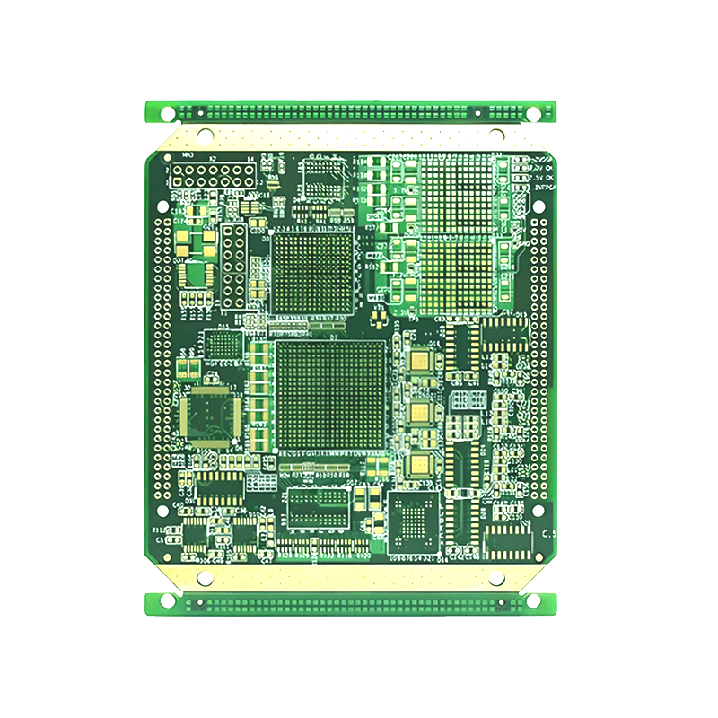
-Edge positioning hole: located at the edge of the PCB board (usually in the corner or edge), making it easy for equipment or fixtures to grasp and position from the board edge, commonly seen in standardized PCBs produced in bulk.
-Internal positioning hole: located in the non edge area inside the PCB, suitable for scenarios where there is no space on the board edge or special positioning is required (such as auxiliary positioning in the middle area of large PCBs).
Ⅲ. The core function of positioning holes
The role of positioning holes runs through the entire lifecycle of PCB, with the core being to solve the two major problems of “precise alignment” and “stable fixation”, as follows:
1. Ensure production accuracy: In the processes of PCB manufacturing such as pressing, exposure, etching, etc., positioning holes are used to ensure precise alignment of the graphics and hole positions in each link, avoiding defects such as interlayer misalignment and circuit offset. This is the foundation of multi-layer board and high-precision PCB production.
2. Improve assembly reliability: During SMT or plug-in stages, positioning holes provide coordinate benchmarks for equipment, ensuring accurate placement/insertion of components and reducing assembly defects such as virtual soldering and wrong soldering.
3. Ensure testing accuracy: During testing, the relative position between the PCB and the fixture is fixed through positioning holes to ensure accurate contact between the probe and the testing point, avoid testing errors, and improve testing efficiency.
4. Auxiliary mechanical fixation: Some positioning holes can also serve as installation holes. When assembling the final product (such as fixing the PCB to the shell/bracket), mechanical fixation can be achieved by using screws or other matching positioning holes to ensure the stability of the overall structure.
Summarize
Positioning holes are “implicit but critical” elements in PCB design, and their types and designs need to be determined based on specific production, assembly, and testing requirements, directly affecting the accuracy, yield, and reliability of the PCB. Reasonable positioning hole design can significantly reduce errors in production and assembly, and is one of the core guarantees for PCB industrial production.
Get your exclusive quote immediately: fill out the form or send an email directly.As a professional PCB manufacturer for hobbyist , we will provide you with a quote service within 24 hours. Enjoy free DFM optimization and a 10% discount on SMT patches for your first order!