High reliability circuit boards (such as those used in aerospace, military, medical, industrial control, and other fields) need to maintain stable performance in extreme environments and long-term operation. Their core characteristics revolve around “reducing the risk of failure, resisting environmental interference, extending lifespan, and ensuring functional continuity”. Here are 10 important characteristics:
Table of Contents
1. High stability substrate and material selection
The performance of the substrate and auxiliary materials directly determines the basic reliability of the circuit board.
-Substrate: Made of high glass transition temperature (Tg ≥ 170 ℃) copper-clad laminates (such as FR-4 high Tg, polyimide), which are resistant to high temperatures (welding or working environment) and are not easily deformed or delaminated; Select low loss substrates (such as PTFE) for high-frequency scenarios to reduce signal attenuation.

-Copper coating and plating: Use high-purity electrolytic copper (purity ≥ 99.9%), with a copper coating thickness ≥ 1oz (to enhance current carrying capacity and mechanical strength); The solder pads are coated with wear-resistant/anti-oxidation coatings (such as chemical nickel gold ENIG, hard gold) to reduce the risk of solder joint oxidation.
-Solder resist layer: Choose solder resist ink that is resistant to high temperatures and chemical corrosion (such as UV curing type) to prevent short circuits between solder pads and environmental erosion.
2. Redundant and fault-tolerant design
Avoiding system crashes caused by single point failures through “backup” and “fault isolation”.
-Functional redundancy: Key circuits (such as power supply, clock, communication interface) are designed with dual primary and backup circuits, and automatic switching (such as power module hot backup) is achieved; The core chip uses memory with ECC (Error Correction) to correct data errors.
-Structural redundancy: Important signal lines adopt “dual line parallel+cross validation”, even if a single line is disconnected, the signal can still be restored through validation; Redundant connector pins (such as multi pin grounding) to reduce the impact of poor contact.
-Fault self detection: Integrated sensors (such as temperature and voltage monitoring) and diagnostic circuits, real-time detection of abnormalities and triggering protection (such as power outage, switching to backup).
3. Wide environmental adaptability
Capable of withstanding harsh conditions such as extreme temperature, humidity, and vibration.
-High and low temperature tolerance: The working temperature range covers -55 ℃~125 ℃ (industrial grade) or -65 ℃~150 ℃ (military grade), and the substrate and components have no performance drift (such as capacitance change ≤ 10%, resistance accuracy maintained ± 1%).
-Moisture resistance and anti condensation: Certified with IPC-6012 Moisture Sensitivity Level (MSL) Level 1, it operates stably in a 95% RH (no condensation) environment to avoid insulation degradation caused by substrate moisture absorption.
-Anti vibration and impact: Complies with MIL-STD-883H or IEC 60068-2-6 standards, with no solder joint detachment or component loosening at vibration frequencies of 10-2000Hz; When the impact acceleration is ≥ 500G (1ms), the structure is intact.
4. Excellent EMI/EMC performance
Reduce the impact of electromagnetic interference (EMI) on the outside world while resisting external electromagnetic interference (EMC).
-EMI suppression: Key signal lines (such as clock and high-speed data) are designed with shielding layers (wrapped in copper foil) or differential pairs (such as USB and LVDS) to reduce radiation; Add a π – type filter (inductor+capacitor) to the power input terminal to suppress conducted interference.
-EMC anti-interference: Sensitive circuits (such as sensor signal chains) should be kept away from power devices (such as MOSFETs, transformers), or isolated by grounding (such as separating analog ground from digital ground, single point connection); Add TVS tubes and magnetic beads to the interface to absorb surges and pulse interference.
-Grounding optimization: Using a large area ground plane (GND Plane) to reduce grounding impedance and quickly discharge interference current.
5. High reliability solder joints and interconnects
Solder joints are weak links in mechanical and electrical connections, and their durability needs to be strengthened.

-Welding process: lead-free high-temperature solder (such as SAC305, melting point 217 ℃) is used to avoid low-temperature solder (such as Sn Pb) softening at high temperatures; Key solder joints (such as BGA and QFP) are subjected to reflow soldering and X-ray inspection to ensure that the solder balls are full and free of voids (void rate ≤ 5%).
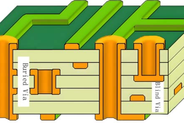
-Through hole and via design: The via adopts the “plug hole+copper plating” process to enhance mechanical strength; The plug-in pins adopt “through-hole reflow soldering” (THR), with solder joints wrapping the pin length ≥ 2mm, and the anti vibration ability is improved by 30%.
-Thermal stress relief: Install thermal conductive adhesive at the bottom of large-sized components (such as transformers and capacitors) to reduce fatigue cracking of solder joints caused by temperature cycling (-40 ℃~125 ℃, 1000 cycles).
6. Comprehensive over stress protection
Resist transient stresses such as overvoltage, overcurrent, and overheating to prevent component damage.
-Overvoltage protection: Add TVS tube (response time ≤ 1ns) and varistor at the power inlet to absorb lightning strikes or grid surges (such as meeting IEC 61000-4-5, withstand 2kV/10kV impact); Add LDO or current limiting chip to the chip power supply end to prevent voltage spikes.
-Overcurrent protection: The critical circuit is connected in series with PTC self recovery fuses or fuses (such as 125 ℃ rated temperature), which quickly cut off in case of overcurrent (response time ≤ 100ms), and automatically recover after troubleshooting.
-Over temperature protection: NTC thermistor is attached next to power devices (such as MCU, power transistor), and when the temperature exceeds the threshold (such as 150 ℃), it triggers power-off or derating operation; PCB layout should be kept away from heat sources to avoid local hotspots (temperature difference ≤ 10 ℃).
7. Selection of long-life components
The aging of components is a reliability weakness, and high durability models should be prioritized.
-Grade selection: Industrial grade (-40 ℃~85 ℃) or military grade (-55 ℃~125 ℃) is selected for core components (such as MCU, operational amplifier), and consumer grade devices are rejected; Electrolytic capacitors are selected with a long lifespan (such as 10000 hours at 105 ℃), and their lifespan is extended by reducing the ripple current rating (≤ 70% of the rated value).
-Passive components: Resistors are made of metal film (accuracy ± 0.1%, temperature drift ≤ 25ppm/℃) instead of carbon film; Shielded magnetic cores are used for inductors to reduce magnetic saturation; Ceramic capacitors are made of C0G/NP0 material, with a capacity temperature drift of ≤ 30ppm/℃.
-Connector: Select industrial grade connectors (such as M12, D-sub) with locking structures (such as buckles and screws), with a plug-in life of ≥ 1000 times and a contact resistance of ≤ 10m Ω.
8. Enhanced Signal Integrity (SI)
Ensure stable transmission of high-speed/high-frequency signals to avoid errors or functional failures.
-Impedance matching: High speed signal lines (such as DDR, PCIe) strictly control the characteristic impedance (such as 50 Ω, 100 Ω), optimize the line width, line spacing, and reference plane through simulation, and achieve impedance deviation of ≤± 10%.
-Crosstalk suppression: The distance between adjacent signal lines is ≥ 3 times the line width, and a grounding isolation band is added between sensitive signals (such as analog signals) and high-speed digital lines; Differential length difference ≤ 5mil to reduce timing offset.
-Signal integrity testing: Before mass production, impedance continuity is tested using TDR (Time Domain Reflectometer), and eye diagram testing verifies that high-speed signals (such as 10Gbps or above) have no inter symbol interference.
9. Corrosion prevention and environmental isolation
Resist erosion from moisture, chemicals, dust, etc., and extend service life.
-Surface treatment: The PCB is coated with a three proof paint (such as silicone rubber, acrylic) with a thickness of 50-100 μ m, covering the pins and solder joints of the components. It has passed IPC-CC-830 certification and is resistant to salt spray for ≥ 500 hours (ASTM B117 standard).
-Sealing design: Key areas (such as connectors and sensor interfaces) are sealed with sealing rings or potting glue (such as epoxy resin) to achieve IP67 protection level, preventing liquids and dust from entering.
-Anti electrochemical corrosion: Avoid direct contact between different metals (such as copper and aluminum) (with coating isolation) to prevent corrosion caused by the formation of primary batteries in humid environments.
10. Strict manufacturing and testing control
Ensure consistency and absence of potential defects through process control and reliability testing.
-Process control: Monitor the entire manufacturing process (such as AOI detection of pad defects, ATE testing of circuit connectivity), and control the accuracy of key processes (such as drilling and electroplating) within ± 0.01mm; Batch yield ≥ 99.5% to avoid early failure.
-Reliability testing: HALT (High Acceleration Life Test) is performed on each batch of samples to quickly expose potential defects through high and low temperature cycling, vibration, and voltage stress; Key products need to pass HTOL (high-temperature working life test, 1000 hours at 125 ℃) and THB (temperature and humidity bias test, 85 ℃/85% RH, 1000 hours).
-Traceability: Record information such as substrate batch, component model/batch number, manufacturing time, etc., to facilitate later fault analysis and traceability, and support continuous improvement.
These characteristics are interrelated and jointly ensure the stable operation of the circuit board in long-term and harsh environments. The design core of high reliability circuit boards is “predicting risks – active protection – testing and verification”, ultimately achieving the goal of “low failure efficiency (such as<100 FIT, which means 1 billion hours of failure times<100)”.
Get your exclusive quote immediately: fill out the form or send an email directly.As a professional PCB manufacturer for hobbyist , we will provide you with a quote service within 24 hours. Enjoy free DFM optimization and a 10% discount on SMT patches for your first order!