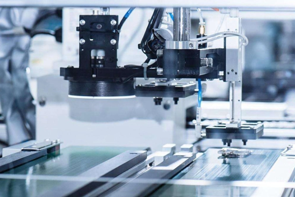
Flying pin testing is a non-contact electrical testing technique used for PCB (printed circuit board) and electronic components. It detects electrical performance such as conductivity, short circuit, and open circuit by contacting the circuit board pads or test points with thin pins (probes). Analyze its advantages and disadvantages from multiple dimensions as follows:
Table of Contents
1、 The advantages of flying needle testing
1. High flexibility, adaptable to diverse needs
-No need for customized fixtures: Traditional needle bed testing requires specialized fixtures designed for each PCB (high cost, long cycle), while flying needle testing can quickly adapt to different PCB patterns and sizes through computer-controlled probe movement, especially suitable for small batches and multiple varieties of products (such as research and development samples, customized circuit boards).

-Supporting complex structures: capable of testing high-density PCBs (such as BGA, fine pitch solder pads), irregular boards, or circuit boards with obstacles (uneven component heights), probes can flexibly avoid the component body and contact concealed testing points.
2. Significant cost-effectiveness, suitable for small batch scenarios
-Low initial investment: No need for expensive customized fixtures, equipment costs mainly focus on probe robotic arms and control systems, making it more economical for small-scale production or research and development stages.
-Low maintenance cost: Probe wear and tear can be replaced separately, without the need for overall maintenance like needle bed fixtures, resulting in lower long-term usage costs.
3. High testing accuracy, covering detailed scenes
-High precision contact: The probe diameter is usually 0.1~0.3mm, which can contact small solder pads (such as the solder pads of 01005 packaged components), and the detection accuracy reaches microampere level current and millivolt level voltage, suitable for precision circuit testing.
-Support dynamic testing: It can simulate signal input and output while powered on to test circuit functions (such as logic levels and timing characteristics), rather than just static conductivity detection.
4. Non destructive testing to protect circuit boards
-The probe pressure is controllable (usually<10g), and the wear of the solder pad is much lower than that of the needle bed test (the fixed needle pressure of the needle bed fixture is relatively high, and long-term use may damage the solder pad). It is suitable for high reliability or circuit boards that require multiple tests (such as repair boards).
5. Convenient programming and support for automation
-The testing program can be directly imported through CAD files (such as Gerber) or PCB design software, without the need for complex manual wiring, and can be integrated with production line automation systems (such as AOI, SPI) to improve testing efficiency.
2、 Disadvantages of Flying Needle Testing
1. Slow testing speed, not suitable for mass production

-Point by point testing characteristics: Flying needle testing requires a robotic arm to move probes to detect each point (usually 4-8 probes work simultaneously), while needle bed testing can contact all test points at once. Flying needles are significantly less efficient in mass production than needle beds (such as testing a PCB, flying needles may take several minutes, while needle beds only take a few seconds).
-Mobile time consumption: The movement and positioning of the probe between different testing points takes time, especially when the distribution of testing points is scattered, the efficiency is further reduced.
2. Limited coverage of complex circuits, relying on test point design
-Test points need to be reserved: For multi-layer boards or complex circuits, if sufficient test points are not reserved during design (such as test points for the inner network), flying needles may not be able to detect deep short circuits or open circuits, while needle beds can contact the inner network through through through holes.
-Unable to test embedded components: For components embedded inside the PCB (such as buried resistors and capacitors), flying pins cannot directly contact them and rely on peripheral circuit testing, which may have blind spots.
3. Hardware limitations, not suitable for high-power or high-frequency circuits
-Low current/voltage carrying capacity: The contact resistance of the probe is relatively high (usually in the milliohm range), making it unsuitable for testing high currents (such as power modules) or high-frequency signals (which may cause impedance matching problems and affect testing accuracy).
-High frequency signal interference: The flying needle test line is relatively long, which can easily introduce noise in the high-frequency circuit, resulting in test result deviation. However, the needle bed fixture can reduce interference by short circuiting.

4. High equipment costs and maintenance requirements
-High end equipment prices: The cost of high-precision flying needle testing equipment (such as multi probe and dynamic testing functions) can reach hundreds of thousands of dollars, which is lower than the long-term cost of needle bed fixtures, but the initial investment is still relatively high.
-High maintenance technical requirements: Probe positioning systems (such as servo motors and optical recognition) need to be calibrated regularly. If there is mechanical wear or software failure, maintenance is difficult.
5. There are requirements for PCB design, and compatibility is limited
-Test point spacing limitation: The probe movement accuracy is about ± 50 μ m, and the test point spacing needs to be ≥ 0.2mm, otherwise probe collision or poor contact may occur. The test point spacing of high-density PCBs (such as mobile phone motherboards) may be smaller and require special design.
-Flatness requirement for board surface: The PCB warpage should be less than 0.5mm, otherwise the probe may not be able to accurately contact due to height deviation, and the needle bed fixture can adaptively warp the board through pressure.
3、 Comparison of application scenarios
| Scenario | Advantages of Flying Needle Testing | More Suitable Testing Methods |
| R&D stage | Quickly validate sample circuits without waiting for fixture production | Flying needle testing |
| Small batch production | Multiple varieties, small batch PCBs, low cost, flexible adjustment | Flying needle testing |
| Mass production | Low efficiency, not recommended | Needle bed testing (such as ICT) or automated online testing |
| Precision/high-density board | Suitable for small testing points, non-destructive testing | Flying needle testing+AOI (automatic optical inspection) combined |
| Power/high-frequency circuits | Not suitable for (current/signal interference issues) | Dedicated power testing equipment or high-frequency network analyzer |
4、 Summary
Flying needle testing has the core advantages of “flexibility” and “high precision”, making it particularly suitable for electrical testing of research and development, small batches, and precision circuit boards. However, due to speed and hardware characteristics, its application in large-scale production and special circuits (power, high frequency) is limited. In actual production, flying needle testing is often combined with needle bed testing (ICT) and automatic optical inspection (AOI) to complement each other and cover the testing needs of different scenarios. With the development of technology, technologies such as multi probe parallel testing and laser positioning are gradually improving the speed of flying needle testing, but their essential characteristics still determine their auxiliary positioning in large-scale production.
Get your exclusive quote immediately: fill out the form or send an email directly.As a professional PCB manufacturer for hobbyist , we will provide you with a quote service within 24 hours. Enjoy free DFM optimization and a 10% discount on SMT patches for your first order!