The line width of a PCB trace is the width of the copper path that connects different components. It is crucial for carrying current between those components. If the trace is too narrow for the amount of current it needs to carry, it can heat up and even burn out, resulting in potential failure of the circuit. On the other hand, if the trace is too wide, it can unnecessarily increase the board’s size, add cost, and reduce manufacturing efficiency.
Table of Contents
Standard Guidelines for PCB Trace Width Calculation
To design PCBs with reliable current carrying capacity, PCB designers use a general guideline called the IPC-2221 standard or specialized trace width calculators. The IPC-2221 standard provides equations to determine the proper trace width based on factors such as current, temperature rise, and copper thickness. However, here are some simplified recommendations and calculators that can help in the design process.
Trace Width Calculation Formula
A commonly used formula to calculate trace width is:
Where:
W = Trace width in mils (thousandths of an inch)
I = Current in amperes
K = A constant that depends on the copper thickness (typically 0.048 for 1 oz/ft² copper)
ΔT = Maximum temperature rise in degrees Celsius (typically 10-30°C)
T = Copper thickness in mils (e.g., 1 oz copper = 1.4 mils)
For practical purposes, however, many designers use online calculators or software like PCBWay’s Trace Width Calculator or Advanced Circuits’ Trace Width Calculator to quickly determine the necessary trace width for their designs.
Current Capacity and Trace Width
To give you a better idea of the relationship between current and trace width, let’s consider some typical scenarios for 1 oz copper (the most commonly used copper thickness in PCB fabrication) with a temperature rise of 10°C:
| Current (Amps) | Trace Width (mil) |
| 1 A | 10 mil |
| 2 A | 15 mil |
| 5 A | 30 mil |
| 10 A | 60 mil |
| 20 A | 100 mil |
| 30 A | 130 mil |
For high current applications, such as power supplies, LED circuits, and motor drivers, trace width must be carefully designed to handle the increased current without excessive heating or voltage drop.
Factors Affecting Trace Width and Current Capacity
While the above table offers a good starting point, there are several other important factors to consider when calculating trace width for a PCB:
1. Temperature Rise
The temperature rise in the trace is critical for determining how much current it can handle. Most PCB designs are aimed at limiting the temperature rise to around 10°C to 30°C. The higher the current passing through a trace, the more heat it generates. For instance, a higher temperature rise requires wider traces to dissipate the generated heat effectively.
In some applications, like power circuits or in automotive electronics, managing heat dissipation is a more complex challenge, requiring considerations for active cooling or heatsinks to maintain safe operating temperatures.
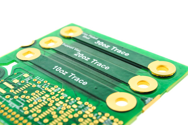
2. Copper Thickness
Standard copper thickness for most PCBs is 1 oz per square foot (1 oz/ft²), but in high-current applications, thicker copper may be used to increase the current capacity of the trace. For example:
2 oz/ft² copper increases the current capacity by about 40%.
3 oz/ft² copper can handle about 60% more current compared to 1 oz copper.
Thicker copper allows traces to carry more current and reduces the temperature rise, but it also increases the cost and complexity of the manufacturing process.
3. Trace Length
Longer traces experience more resistance, leading to increased voltage drop and potential heat buildup. For long power traces, you may need to increase the width of the trace or use thicker copper to accommodate the current safely. Additionally, you might consider using vias to add multiple paths for current flow and reduce resistance.
4. Multilayer PCBs and Internal Layers
For multilayer PCBs, internal traces are often smaller because the power distribution is handled by thicker planes on the internal layers. The outer layers still require the trace width calculation for surface-mounted components, but internal traces usually carry less current due to the availability of power planes.
5. High-Speed Circuits
In high-speed digital circuits, controlling impedance becomes a critical factor, and the trace width must be designed to achieve the required impedance. This will often conflict with the need for wider traces to handle higher current, requiring designers to balance power and signal integrity.
6. Heat Management
If the PCB design involves a lot of high-current pathways, efficient heat management is crucial. This could include using heat sinks, thermal vias, and distributed heat management strategies to ensure that the trace widths are designed for both electrical performance and thermal management.
Practical Tips for Ensuring Safe Trace Widths
Use a Reliable Calculator: There are many online tools and PCB design software (like Altium Designer or KiCad) that have built-in trace width calculators. These tools can save time and ensure that your calculations are accurate.
Account for Tolerance: Always include a tolerance margin when designing trace widths, especially for critical applications. A slight variation in trace width can have significant implications for the performance of the circuit.
Design for Safety: When in doubt, choose wider traces. It’s easier to shrink down traces later in the design phase than to make them wider after manufacturing.
Plan for Thermal Management: Ensure that the board’s thermal management system is capable of dissipating heat from high-current traces effectively. Consider using thermal vias, heatsinks, or even active cooling for high-power applications.
Follow IPC Standards: Adhering to standards like IPC-2221 ensures that your PCB design will be reliable, manufacturable, and compliant with industry best practices.
Conclusion
Determining the appropriate trace width for a PCB is a crucial aspect of designing reliable, high-performance electronic systems. By understanding the relationship between current, trace width, and copper thickness, and by considering factors such as temperature rise and trace length, you can design PCBs that ensure both electrical functionality and thermal safety. Properly calculated trace widths help prevent overheating, signal integrity issues, and potential failures, leading to more durable and efficient electronic products.