In the era of the Internet of Things, ESP8266 has become the “nerve endings” of global IoT devices due to its three major characteristics of low cost, high integration, and low power consumption. As a PCB enterprise, a deep understanding of its technical characteristics and application scenarios is crucial for designing high reliability IoT hardware. This article will analyze chip performance, typical applications, PCB design challenges, and future trends, providing technical references for industry partners.
Table of Contents
1、 The core advantage of ESP8266: redefining IoT access
1. Full stack integration, breaking the cost limit
The ESP8266 integrates a 32-bit Tensilica processor, TCP/IP protocol stack, Wi Fi RF module, and rich peripheral interfaces, allowing for network connectivity and data processing on a single chip, significantly reducing BOM costs. Its module price is only one-third of traditional Wi Fi solutions, promoting the popularization of smart hardware.
2. Precise power consumption control, increased battery life
Supports four levels of power consumption mode:
-Deep sleep (10 μ A): Only RTC operation, suitable for battery powered sensors;
-Mild sleep (0.9mA): CPU paused, Wi Fi turned off, fast wake-up;
-Activity mode (70-170mA): Fully functional operation, reducing peak power consumption through dynamic frequency modulation.
For example, smart agricultural sensors can work for several years in deep sleep mode, only requiring timed wake-up to upload data.
3. Development friendly and ecologically mature
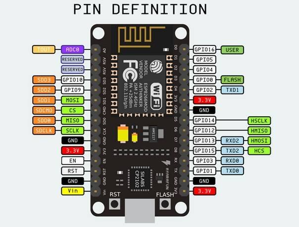
-At the software level, it supports development environments such as Arduino and MicroPython, and simplifies network configuration with the AT instruction set (such as setting dual-mode connection with AT+CWMOD=3);
-At the hardware level, we offer over 10 different packaging options, including ESP-01 to ESP-12F, to meet varying complexity requirements (Table 1).
Table 1: Selection Guide for Mainstream ESP8266 Modules
| Model | Size (mm) | GPIO Number | Antenna Type | Applicable Scenarios |
| ESP-01 | 14 × 24 | 2 | PCB antenna | Simple switch type equipment (such as smart lights) |
| ESP-12F | 24 × 16 | 22 | Ceramic antenna+external interface | Multi sensor gateway, industrial controller |
| Wemos D1 | 34 × 26 | 11 | PCB antenna | Prototype development, small and medium batch production |
2、 Application scenario: From smart homes to the practical implementation of Industry 4.0
1. Smart Home: Balancing Safety and Experience
-Magnetic safety socket: connected to Xiaomi smart home through ESP8266, combined with NE555 square wave authentication circuit, to achieve plug suction detection before power on, avoiding the risk of electric shock and providing barrier free operation experience for visually impaired people;
-Temperature and humidity linkage system: STM32+ESP8266 combination solution, data uploaded to OneNet cloud platform, users can remotely adjust PWM light brightness, response delay<200ms.

2. Industrial monitoring: breakthroughs in reliability and real-time performance
-Motor status monitoring: The ESP-07 module is equipped with an external high gain antenna, which maintains a signal strength of -80dBm in the complex electromagnetic environment of the workshop. Vibration data is transmitted to the cloud platform through the MQTT protocol;
-Agricultural irrigation network: ESP-12F drives soil moisture sensors, with a daily power consumption of<1mAh in deep sleep mode, and solar panels provide sustainable power supply.
3. Innovative healthcare: miniaturization and biocompatible design
The hearing aid is equipped with an ESP8266 module, which uses rigid flex and PCB to achieve ear canal surface fitting. Data is transmitted through low-power Bluetooth to reduce the impact of radio frequency radiation on the human body.
3、 Key Technologies in PCB Design: The Foundation of Highly Reliable IoT Devices
1. RF layout: the lifeline of signal integrity
-Antenna clearance area: A copper free area of ≥ 3mm is reserved around the ceramic antenna to avoid parasitic capacitance interference from the copper coating;
-Impedance matching: Designed with a 50 Ω microstrip line, with a differential length tolerance of ± 0.1mm, ensuring a 2.4GHz frequency band return loss of<-15dB.
2. Power integrity: solving the problem of surge and noise
-Three level filtering architecture: input stage TVS tube surge protection+intermediate stage LC π – type filtering+chip end 0.1 μ F/10 μ F capacitor decoupling;
-Power supply selection: Disable LDO (efficiency<60%), recommend using DC-DC converter (such as SY8088), conversion efficiency>92%.

3. Thermal management and structural optimization
-Metal substrate heat dissipation: Aluminum substrate has a thermal conductivity of 2.0W/m · K, which is four times higher than FR-4, solving the problem of temperature rise in dense layouts (such as LED driver circuits);
-Splicing design: V-Cut+stamp hole composite technology to improve the production yield of micro modules such as ESP-01.
4、 Future trend: AIoT integration and green manufacturing
1. Edge intelligence upgrade
ESP8266 has started integrating lightweight AI frameworks such as TinyML, supporting local speech recognition and reducing cloud dependence. For example, the smart switch responds to commands through local keyword recognition, reducing standby power consumption to 1mW.
2. Green materials and processes
-Halogen free substrate: Made of Shengyi Technology S1165 board, with a flame retardancy of UL94 V0 level and a 50% reduction in ion migration rate;
-Waste liquid circulation system: Etching solution online regeneration technology, copper recovery rate>90%, in line with ESG standards.
3. Security architecture enhancement
The hardware encryption engine supports AES-256, combined with Secure Boot to prevent firmware tampering, meeting the financial level security requirements of scenarios such as smart meters.
Conclusion
ESP8266 is not only a bridge connecting the physical and digital worlds, but also a touchstone for PCB technology innovation. From RF design to power control, from flexible circuits to green manufacturing, every detail concerns the life and death of IoT terminals. As a PCB company, we need to continuously cultivate high-frequency materials, high-density interconnects, and signal integrity technologies to provide the hardware foundation for “reliable connections” in the trillion dollar IoT market. When everything can be connected, only ultimate craftsmanship can intelligently connect the future.