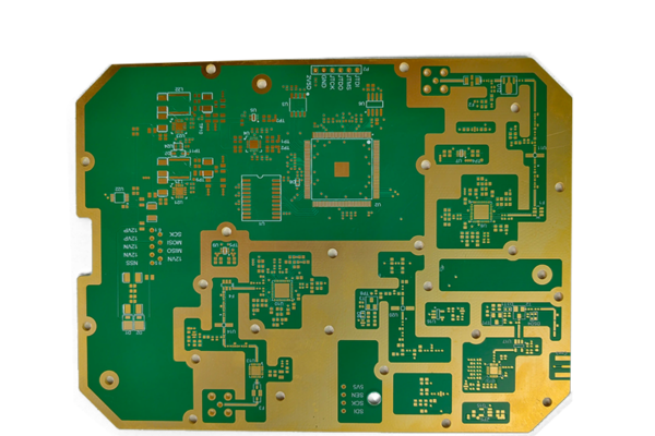
There are 3 different types of vias in A HDI PCB. Through vias which from surface to surface, blind vias from surface to inner layer, buried vias from inner layer to inner layer.
Shenzhen China PCB manufacturer give a brief introduction of HDI boards. High Density Interconnection PCB, using the technology of blind vias less than 6mil, is one of the fastest growing technologies in PCBs field, are now available at Shenzhen SysPCB. HDI Boards have a higher circuitry density than traditional PCB boards.

Manufacturing HDI boards requires advanced equipment and special processes such as laser drills, plugging, sequential lamination cycles and conformal laser drill. HDI PCBs normally have small lines/space and small annular ring, it requires a significant investment in equipment and additional time in producing processes.
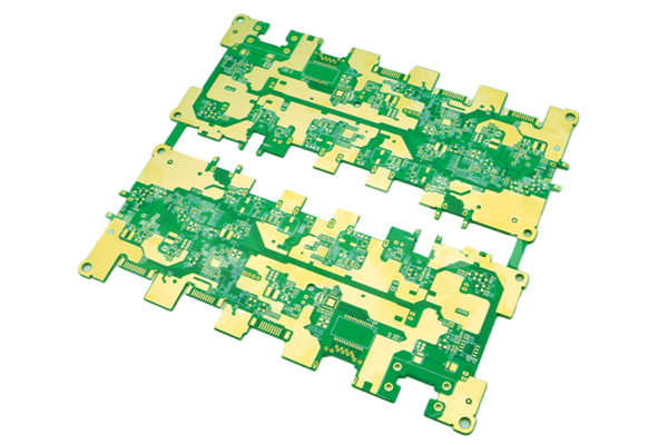
Using HDI technology in PCB layout, it is possible to reduce an 8 layer through-hole PCB to a 4 layer HDI microvia technology PCB. The solder capabilities of a well-designed HDI 4 layer PCB can achieve the same or better functions as that of a standard 8 layer PCB.
Via in Pad Technology-Vias are plated through with copper and then filled with conductive or non-conductive material. These vias are finally plated over with copper. Via in Pad can save PCB spacing and also provides a direct conduit for heat transfer.
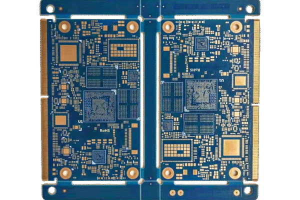
With HDI Technology, electric products can achieve more function, weigh less and be physically smaller. Specialty equipment, mini-components and thinner materials have allowed for electronics to shrink in size while expanding technology, quality and speed.