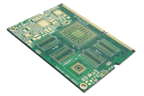
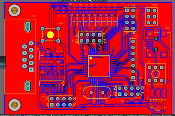
Printed circuit board can generally be divided into two parts, the substrate (normally prepreg) and copper conductive layer. Wherein the conductive line layers we using copper foil, also known as copper sheet, copper covering the both surface of prepreg. These 2 copper conductive layers are the core of the entire PCB. Designers use variety of design software to make the schematic layout, after circuit designed, according to the design drawings, by using special photographic machines, exposing and etching of copper layer, etch out the unwanted parts to form a complete copper layer. Then we can see the lines and pads on the conductive layer.
What is the layer account of PCB board?
In general, PCB board has two outer layers, which are located in the upper and lower surfaces of the PCB, the circuit line on the top and bottom are different. Because the electric needs and safety consideration of the circuit design, such as power layer and ground layer, usually on a separate inner layer.

In some special circumstances, for some complex circuits, one may not be able to arranged for all of the lines in just one layer or one layer can not be arranged for the precise control of the circuit (certain parts has a very fine on request of the impedance control).
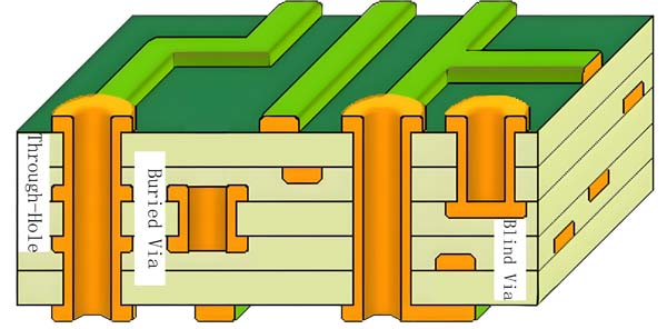
Then you need to use multiple layers for PCB. Multi-layer PCB is actually the single layer PCB laminated together so that the different conductive layer can be designed to meet the needs of complex circuits, Conventional FR4 PCB is generally divided into two layer, 4 layers , 6 layers, 8 layers, 10 layer etc.
How to choose the PCB by Layer when ordering PCB?
First of all, just according to the customer’s business needs to define how many layers the PCB is. For example, a customer want to manufacture a motherboard graphics board, it was just a small part of the purchase, because before mass production of the circuit boards, we will certainly test reliability of the PCB. Even using a 4 layer or even 2 layer PCB, it certainly is possible to achieve product performance requirements. Because most of the PCB buyers don’t know how to identify the layer account of a PCB, it is not of big use choosing PCB layer in purchasing.


