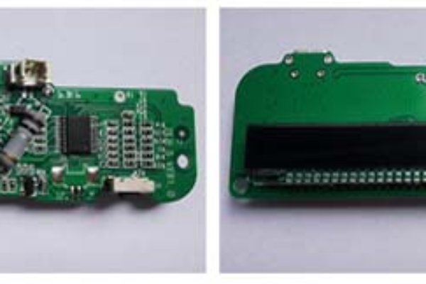
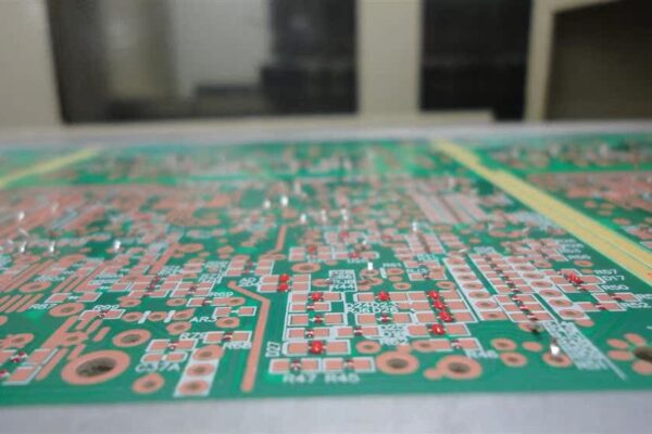
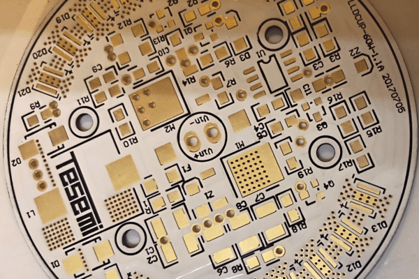
First, the selection of test points:
1. Try to avoid the needle on both sides of the fixture, it is best to put the test points on the same side.
2. The test points are selected in order of priority (See Appendix A for details): Test point – DIP – VIA – SMT
Second, the test point:
1. The distance between the two test points or the test point and the center of the pre-drilled hole is preferably not less than 0.050″ (1.27mm). It is preferably greater than 0.100″ (2.54mm), followed by 0.075″ (1.905mm).
2. The test point should be at least 0.100″ from the nearby parts (on the same side), and at least 0.120″ if it is higher than 3m/m.
3. The test points should be evenly distributed on the surface of the PCB to avoid excessive local density.
4. The diameter of the test point is preferably not less than 0.035″ (0.9mm). If it is on the upper needle plate, it is preferably not less than 0.040″ (1.00mm).
5. The shape is better in square (the measurable area is increased by 21% compared with the circle).
6. Pad and Via of the test point should not have Solder Mask.
7. The test point should be at least 0.100″ from the edge of the board.
8. Try to avoid placing the test point on the SMT part because the contact tin surface is too small and it is easy to crush the part.
9. Try to avoid using too long part feet (greater than 0.170″ (4.3mm)) or too large aperture (greater than 1.5mm) as the test point, which requires special treatment.
Third, the tooling hole:
1. The PCB to be tested must have 2 or more tooling holes, and the holes should not be tinned. The position is preferably at the opposite corner of the PCB.
2. The tooling hole is selected as the diagonal line, and the two holes that are furthest away are the tooling holes.
3. The tolerance of the test point to the tooling hole should be +/-0.002″.
4. The diameter of the Tooling Hole is preferably 0.125″ (3.175mm) with a tolerance of “+0.002″/-0.001”.
Fourth, other:
Appendix A, test point position consideration order (each copper foil, regardless of shape, at least one testable point required):
The ACI plug-in part foot is prioritized as a test point.
Copper foil exposed part (test PAD), it is best to tin.
Vertical parts plug-in feet.
Through Hole should not have Solder Mask.
Appendix B, test point diameter
1mm or more, with the general probe can achieve the best test results.
Below 1mm, must use more precise probes, and the manufacturing cost will increase.
The spacing between points is preferably greater than 2 mm (center point to center point).
Appendix C, double-sided PCB requirements (to be able to make a single-sided test as a key point):
The trace of SMD side must have at least 1 through hole running through the dip side as a test point and tested by the dip side.
If the through hole requires a solder mask, the test pad next to the through hole must be considered.
If it is impossible to make a single side, it will be made by double-sided fixture.
If the empty foot is within the allowable range, the testability should be considered. If there is no test point, the point must be pulled.
Back Up Battery it is best to have a Jumper, which can effectively isolate the circuit during ICT testing.


