In order to standardize the solder paste printing process in the SMT workshop and ensure the quality of solder paste printing, the following process guidelines for solder paste printing in the SMT workshop have been formulated. Today, Shenzhen PCB Assembly factory SYS Tech brought you SMT solder paste printing steps, let’s take a look!
I. Tools and accessories used in SMT solder paste printing process:
1. Printing machine
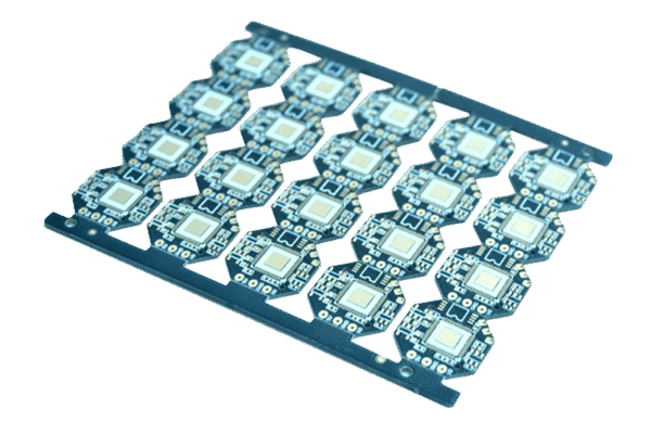
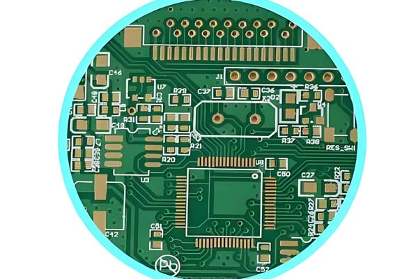
2. PCB board
3. Stencil
4. Solder paste
5. Solder paste mixing knife
II. SMT solder paste printing steps
1. Check before printing
1.1 Check the correctness of the PCB board to be printed;
1.2 Check whether the surface of the PCB to be printed is intact and free of defects and dirt;
1.3 Check whether the stencil is consistent with the PCB and whether its tension meets the printing requirements;
1.4 Check whether the stencil is blocked. If there is a blocking phenomenon, wipe the stencil with a dust-free paper moistened with alcohol, and dry it with an air pressure gun. When using the air pressure gun, keep a distance of 3~5 cm from the stencil;
1.5 Check whether the solder paste used is correct, whether it is used according to the “Storage and Use of Solder Paste”, whether it remarks: pay attention to the temperature recovery time, mixing time, lead-free and leaded distinction, etc.
2. SMT solder paste printing
2.1 Fix the correct stencil to the printing machine and adjust it OK;
2.2 Assemble a clean and good squeegee to the printing machine;
2.3 Use the solder paste mixing knife to add the solder paste to the stencil. For the first time to add solder paste, the height of the solder paste is about 1 CM, and the width is 1.5~2 CM. The length depends on the length of the PCB. Both sides should be about 3 CM longer than the printed area. It should not be too long or too short. After that, add solder paste every two hours, and the amount of tin is about 100 G;
2.4 Put in the PCB board for printing, the first 5PCS board printed requires full inspection. After the printing quality is passed, notify the IPQC for the first inspection. After confirming that the printing quality is normal, notify the production line operator to start production;
2.5 During the normal printing process, the operator needs to check the printing effect every half an hour to see if there are any undesirable phenomena such as poor solder, solder bridge, solder projections, offset, and missing printing. Focus on checking the printing effect of components with too dense pins such as “BGA, QFP, SOP, power strip”, etc;
2.6 The stencil needs to be cleaned once every time 5PCS is printed. If there are components with too dense pins on the PCB board such as “BGA, QFP, SOP, FPC connector”, the cleaning frequency should be increased and cleaned every 3PCS;
2.7 During the production process, if continuous 3PCS printing is found to be bad, you should notify the technician should to adjust; clean the badly printed PCB board. When cleaning poorly printed PCB, do not directly scratch the surface of the PCB with hard objects to prevent scratches on the surface wiring of the PCB. If dealing with PCBs with gold fingers, you should avoid the gold fingers. After repeated wiping with dust-free paper moistened with a little alcohol, use an air pressure gun to blow dry, and check under a magnifying glass. If there is no residue solder paste, then it’s OK;
2.8 During the normal printing process, check whether the solder paste has overflowed regularly, and collect the overflowed solder paste;
2.9 After the production is finished, the auxiliary materials and tools such as solder paste, squeegee, and stencil should be recycled, and the frocks and fixtures should be cleaned;
3. Solder paste printing process requirements
3.1 The main defects of printing are: poor solder, continuous solder, solder projections, offset, missing printing, excess solder, scooped solder, dirty board, etc;
3.2 The printing thickness of the solder paste is the thickness of the stencil -0.02mm~+0.04mm;
3.3 Ensure that after reflow soldering effect is free of defects.