Rapid PCB prototyping is a method that can turn an idea into a new product quickly and efficiently. The result is a new, printed circuit board that can become a new product, even if it takes one stage or more.
Speed and flexibility are important factors in developing a new prototype. It is important to design and tests ideas as quickly and as confidently as possible to address both the competition and customers’ requirements.
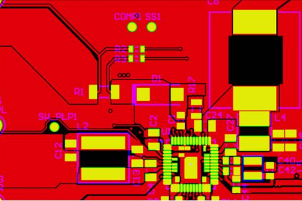
Layout data specific to a particular circuit board prototype is prepared with CAD software. A laser system can plot material on to the circuit board with a particular structure. There is no need for abrasive chemicals to create the new prototype.
PCB prototyping is an essential part in the development of any electronics product. All developed countries have companies and engineers dedicated to prototyping and the process plays an important role in technological innovation.
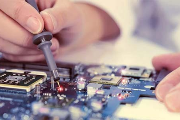
The prototyping process works in a cycle. The initial model, the prototype, is built and tested to ensure that it works according to specifications and expectations. If not, it is designed and rebuilt until an acceptable prototype is achieved. At this stage, the product developers can move on to design and build a whole system.
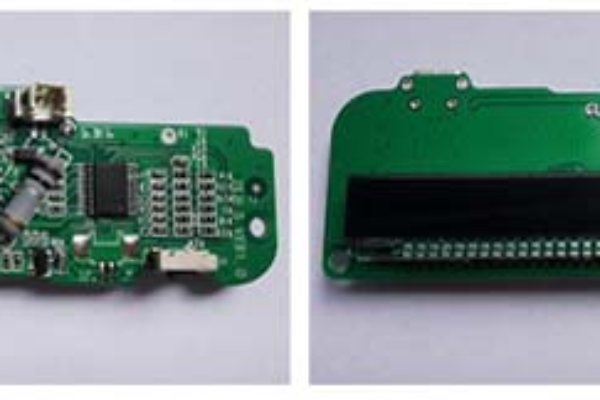
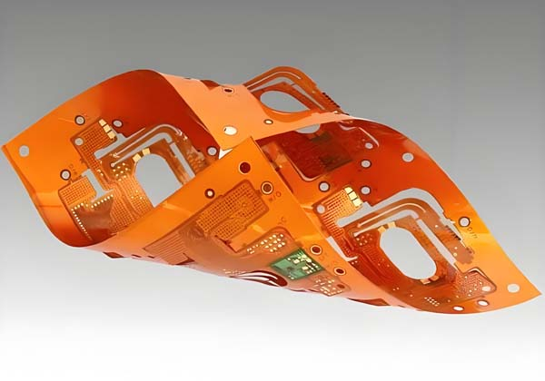
The circuit board can be single or double sided. All of the conducting paths within the circuits on both sides have to be tested to detect faults or any necessary changes to the design.
This is a method that can create a suitable prototype in a few steps. The result is a functioning circuit board that works according to the design requirements. If the results persuade you to think a while and change your ideas, that is not a problem. A new idea can be tested quickly and developed on to the next stage without any worries about expensive research budgets.
With the rapid development of PCB precision processing technology, PCB prototype toward to multilayer PCB prototype design, micro line width and spacing, micro hole, blind& buried hole direction of development. A lot of high frequency communication products of PCB prototype are designed strictly with impedance control, a lot of printing inductance and capacitance. This is a challenge for PCB designers and manufacturers