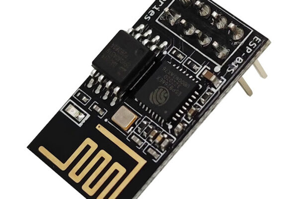
The process requirement of mounting components :
1. The type, model, nominal value and polarity and other characteristics mark of each assembly components should conform to the product’s assembly diagram and detailed table requirement.
2. Mounted components to be without damage.
3. Mounting components solder end or pin not less than 1/2 thickness to immersion the solder paste. For the general components SMD solder paste, extrusion (length) should be less than 0.2mm, for narrow pitch components SMD solder paste, extrusion (length) should be less than 0.1mm.
4. The end or pins of components are aligned with the pad graphics. Because of the self-locating effect when reflowing welding, therefore the component placement position is allowed to have certain deviation.
Allow deviation range requirements are as follows:
(1) rectangular components: under the condition that the PCB solder plate design is correct, the width direction of the components weld end width 3/4 above in the pad, in the length direction of the components the weld end of the components and the pad after overlapping, the solder plate protrudes part to be bigger than 1/3 of the height of the weld end: when there is rotation deviation, the weld end width of the components 3/4 above must be in the pad. Special attention should be paid when mounting: the solder end of the component must be in contact with the solder paste.
(2) Small form factor transistor (SOT): X, Y, T (rotation angle) deviation is allowed, but the pins must all be on the pads.
(3) Small form factor integrated circuit (SOTC): X, Y, T (rotation angle) deviation is allowed, but must ensure that 3/4 of the width of the component pins are on the pads.
(4) Four-sided flat package components and ultra-small package devices (QFP): to ensure that 3/4 of the pin width is on the pad, and allow X, Y, T to have a small placement deviation.
Guarantee the three elements of SMD quality:
1. Correct components require the type, model, nominal value and polarity and other characteristics mark of each assembly components to conform to the product assembly diagram and detailed table requirements, can’t place in the wrong position.
2. Accurate position, the components are in the right position.
(1) The end of the components or pins and pad graphics should be aligned as far as possible, centered, but also to ensure that the components solder contact solder paste.
(2) Component placement position to meet the process requirements. The two ends of Chip components self-locating effect is relatively large, when placing the components width direction 1/2 ~ 3/4 above lap in the pad, length direction two ends as long as lap to the corresponding pad and contact solder paste graphics, in the flow of welding can be self-locating, but if one of the ends did not lap to the pad or no contact solder paste graphics, then flow of welding will produce displacement or hanging bridge; for SOP SOJ, QFP, PLCC and other devices, the self-positioning effect is relatively small, and the placement offset cannot be corrected by reflow soldering. If the placement position exceeds the permissible deviation range, it must be manually corrected and then enter reflow soldering furnace for welding.
Otherwise, after reflow soldering, it must be repaired, which will cause waste of working time and material and even affect the reliability of the product. When the production process finds that the placement position exceeds the allowed range, it should correct the placement coordinates in time. Manual placement or manual dialing is required when the placement position is accurate, the pin is aligned with the pad, centered, do not paste is not allowed, dragging on the solder paste to find the right, one side of the solder paste figure sticking together, cause bridging.
3. Pressure (SMT height) is suitable.
Pressure (Z axis height) should be appropriate and suitable. If the mounting pressure is too small, the component solder end or pin float up the solder paste surface, the solder paste can not stick to the components, in the transfer and reflow soldering prone to have position movement, in addition, because the Z-axis height is too high, when the SMD components throw down from a high position, will cause the SMD position shift.
If the mounting pressure is too big, the solder paste extrusion quantity is too much, it is easy to cause the solder paste sticking together, it is easy to produce the solder bridging when reflowing, at the same time, it will also cause the mounting position offset due to sliding, when serious, it will also damage the components.