Printed circuits, commonly referred to as Printed Circuit Boards (PCBs), are the backbone of nearly all modern electronic devices. From smartphones and laptops to home appliances and industrial machinery, PCBs play a vital role in connecting and supporting electronic components, enabling them to function as cohesive systems. This blog will explore the significance of printed circuits in electronic devices, their structure, manufacturing process, and the role they play in device functionality.
Table of Contents
1. What is a Printed Circuit Board (PCB)?
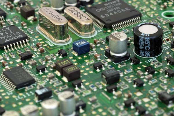
A Printed Circuit Board (PCB) is a flat board made from an insulating material, typically fiberglass or plastic, that provides mechanical support and electrical connections for electronic components. The board is made by etching copper traces onto a non-conductive substrate, forming pathways for electrical signals between components such as resistors, capacitors, diodes, and integrated circuits (ICs). PCBs are essential in ensuring that electronic devices operate efficiently and reliably.
2. What is the structure of PCB?
The structure of a PCB can vary based on the device it is designed for, but it generally includes the following components:
2.1 Substrate (Base Material)
The substrate is the foundation of the PCB and provides mechanical support. The most common substrate materials are fiberglass (FR4), flexible polymers (for flexible PCBs), and ceramics (for high-performance applications). The substrate is usually non-conductive to prevent short circuits.
2.2 Copper Layer
Copper is the conductive material used to form electrical paths on the PCB. After the substrate is manufactured, a thin layer of copper is applied to one or both sides of the board. This copper layer is etched to form the electrical traces, which connect the components.
2.3 Solder Mask
A solder mask is a protective layer applied over the copper traces to prevent oxidation and accidental short circuits. It also prevents solder from bridging between components during the assembly process. The solder mask is often green, but it can come in other colors as well.
2.4 Silkscreen Layer
A silkscreen layer is used to print identifying marks, component labels, and other instructions on the board. This is important for assembly and troubleshooting, as it helps technicians identify the placement and orientation of components.
3. What are the types of printed circuit boards?
PCBs come in different types, designed to meet the requirements of various electronic devices:
3.1 Single-Sided PCBs
Single-sided PCBs have a copper layer on one side of the substrate, with components mounted on the other side. These are simple boards used in low-cost or less complex electronic devices such as calculators or small appliances.
3.2 Double-Sided PCBs
Double-sided PCBs have copper layers on both sides of the substrate. Components can be mounted on both sides, and the electrical connections are made through vias (small holes that are plated with copper). These PCBs are often used in devices that require more complex circuitry but are still cost-effective, such as power supplies and audio equipment.
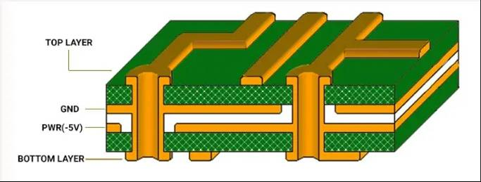
3.3 Multilayer PCBs
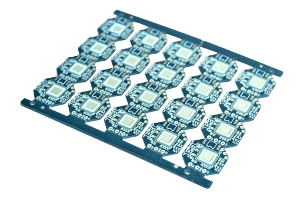
Multilayer PCBs are made up of multiple layers of copper and insulating materials, stacked and laminated together. These boards offer high-density connections and are used in advanced electronic devices such as smartphones, computers, and high-performance industrial machinery. The multiple layers allow for more complex circuits and efficient space utilization.
3.4 Flexible and Rigid-Flexible PCBs
Flexible PCBs can bend and flex, making them ideal for applications where space is limited or where the PCB must conform to a specific shape. Rigid-flex PCBs combine the characteristics of both rigid and flexible boards and are often used in wearable electronics, medical devices, and automotive applications.
4. What is the PCB manufacturing process?
The process of manufacturing PCBs involves several steps, each crucial to ensuring the functionality and quality of the final product. Below is an overview of the typical PCB manufacturing process:
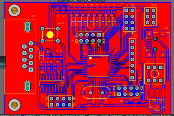
4.1 Design and Schematic Preparation
The first step in PCB manufacturing is the creation of the design. Engineers use PCB design software to create the schematic and layout, which defines how components are connected on the board. The design is then converted into a file format that can be read by PCB fabrication machines.
4.2 Etching and Copper Layering
Once the design is ready, a thin layer of copper is applied to the substrate. The board is then subjected to an etching process, where unwanted copper is removed, leaving behind the desired electrical traces.
4.3 Drilling
If the design includes through-hole components (which need to be mounted on both sides of the PCB), the next step is drilling. Holes are drilled in the PCB to allow components to be inserted and soldered into place.
4.4 Layer Lamination (for Multilayer PCBs)
For multilayer PCBs, individual layers are stacked together and laminated to form a single cohesive board. Special alignment holes ensure that the layers are correctly aligned during the lamination process.
4.5 Solder Mask and Silkscreen Application
After the copper traces are etched, a solder mask is applied to protect the copper from damage. The silkscreen layer is then printed, showing component labels, logos, and other necessary information.
4.6 Component Mounting and Soldering
In this stage, components are placed on the board, either manually or using automated machines. Soldering is then performed to establish permanent electrical connections between the components and the copper traces.
4.7 Testing and Quality Control
Before the PCB is shipped out, it undergoes rigorous testing, including Automated Optical Inspection (AOI), In-Circuit Testing (ICT), and Functional Testing. This ensures that the board is free from defects and operates as expected.
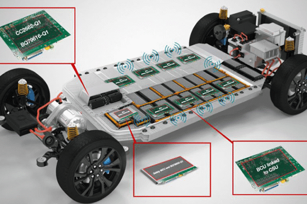
5. What is the role of PCB in electronic devices?
Printed circuit boards are indispensable to electronic devices. They serve as both the physical platform and the electrical pathway for the components to interact. Here’s how PCBs contribute to the performance of electronic devices:
5.1 Electrical Connectivity
PCBs provide the necessary connections between electronic components, enabling them to communicate and function as a unified system. Without PCBs, devices like smartphones, computers, and televisions would not be able to process signals or perform complex operations.
5.2 Space Efficiency
With advancements in PCB technology, manufacturers are able to design more compact and efficient boards, allowing electronic devices to become smaller and more powerful. This is especially important in modern consumer electronics, where miniaturization is key.
5.3 Cost Efficiency
By consolidating complex circuitry onto a single board, PCBs help reduce the size, weight, and cost of electronic devices. This is crucial for mass-market production, where cost-effective solutions are needed without compromising performance.
6. What are the future trends of PCB technology?
The future of printed circuits in electronic devices is evolving rapidly. Some of the emerging trends in PCB technology include:
Flexible and Stretchable PCBs: These are being developed for use in wearable devices and advanced medical applications.
5G and High-Speed PCBs: As the demand for high-speed data transmission grows, PCBs are being designed to support 5G networks and high-frequency applications.
Sustainable PCBs: With increasing awareness of environmental issues, there is a growing focus on developing eco-friendly PCBs, such as those made from recyclable materials or without the use of toxic chemicals.
7. Conclusion
Printed circuits are an essential part of modern electronic devices, providing the structure and electrical connections necessary for the functionality of a wide range of products. With ongoing advancements in PCB technology, we can expect even more compact, efficient, and sustainable solutions in the future. Whether in consumer electronics, medical devices, or industrial machinery, printed circuit boards continue to play a critical role in driving the progress of modern electronics.