The Printed Circuit Board (PCB) is a critical component in modern electronics, serving as the foundation for connecting and supporting electronic components. The manufacturing process of a PCB is complex and involves several stages, each of which is crucial to ensuring the final product is functional, reliable, and of high quality. Below is an overview of the typical PCB manufacturing process, from design to finished product.
1. Design and Schematic Preparation
The first step in the PCB process is the design phase. Engineers use PCB design software such as Altium Designer, Eagle, or KiCAD to create the schematic of the circuit. This schematic serves as a blueprint that dictates the layout of components, their interconnections, and electrical characteristics.
Once the schematic is finalized, the design is converted into a PCB layout. This layout includes the physical positioning of components and the routing of electrical traces that will connect them. The design is verified through Design Rule Checks (DRC) and Electrical Rule Checks (ERC) to ensure there are no errors in the design that could affect performance or manufacturability.
2. PCB Fabrication
Once the design is complete, the next step is the fabrication of the PCB. This involves several sub-steps:
2.1 Material Selection
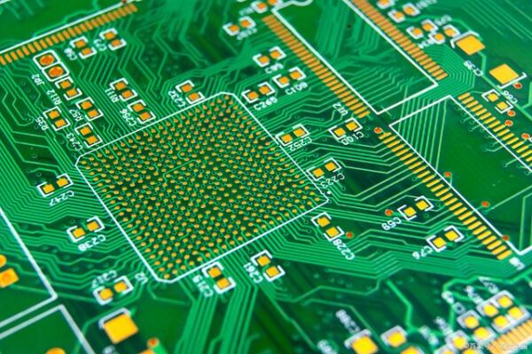
The base material for a PCB is typically copper-clad laminate (CCL), which consists of a non-conductive substrate (usually fiberglass or a similar material) coated with a thin layer of copper. The selection of CCL depends on the application requirements, such as thermal conductivity, flexibility, and electrical properties.
2.2 Printing the Circuit
The PCB design is transferred to the copper-clad laminate through a process called photoengraving. A photoresist layer is applied to the copper surface, and the design is printed onto the board using ultraviolet (UV) light. The photoresist hardens in areas exposed to UV light, while the unexposed areas remain soft. These unexposed areas are then chemically washed away, revealing the copper traces that form the electrical connections.
2.3 Etching
Next, the PCB is subjected to an etching process, where a chemical solution removes excess copper, leaving only the desired traces behind. This creates the electrical pathways on the PCB.
2.4 Drilling Holes
For components that require through-hole mounting (such as resistors, capacitors, and connectors), precise holes are drilled into the PCB. These holes allow the component leads to pass through and be soldered to both sides of the board.
2.5 Plating and Copper Deposition
After drilling, the PCB goes through a plating process. This involves coating the drilled holes with copper to create electrical connections between layers (for multilayer PCBs) or to reinforce the conductive traces.

3. Layer Lamination (for Multilayer PCBs)
For more complex designs, multilayer PCBs are required, which include multiple layers of copper separated by insulating material. These layers are laminated together under heat and pressure to form a solid, multi-layered board. The layers are carefully aligned to ensure accurate electrical connections between them.
4. Solder Mask Application
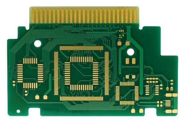
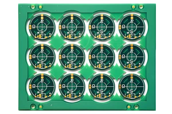
After the PCB’s copper traces are created, a solder mask is applied. The solder mask is a protective layer that prevents solder from bridging between components during assembly and protects the copper traces from oxidation. The solder mask is typically green, although other colors are available.
The mask is applied using a photolithographic process, similar to the etching process, where UV light hardens the mask in specific areas, leaving the pads exposed for component placement.
5. Silkscreen Printing
Once the solder mask is in place, silkscreen printing is used to mark component labels, logos, and other important information on the PCB. This is typically done using an inkjet or screen printing method, where a layer of ink is applied to the surface of the board to indicate component placement and orientation.
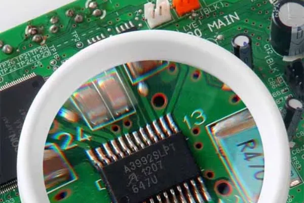
6. Surface Mount Technology (SMT) or Through-Hole Assembly
At this stage, the PCB is ready for component assembly. There are two primary methods for component mounting:
Surface-Mount Technology (SMT): In this method, components are mounted directly onto the surface of the PCB. SMT components are typically smaller and can be placed more densely on the board. A pick-and-place machine is often used to accurately position components on the board.
Through-Hole Technology: For larger components that need to be inserted through holes in the PCB, the leads of the components are passed through the holes and soldered to pads on the other side of the board.
Both methods can be used in tandem on the same PCB, depending on the components’ size and the assembly requirements.
7. Soldering
After the components are placed on the board, they need to be soldered into position. There are two primary soldering methods:
Wave Soldering: This is used for through-hole components, where the PCB is passed over a wave of molten solder.
Reflow Soldering: This method is used for SMT components, where the entire PCB is heated in a reflow oven to melt the solder paste, creating strong and reliable solder joints.
8. Testing and Inspection
After assembly, the PCB undergoes thorough inspection and testing to ensure functionality and quality. Common testing methods include:
Automated Optical Inspection (AOI): Checks for visual defects such as misaligned components, missing parts, or soldering issues.
In-Circuit Testing (ICT): Verifies electrical connections and checks for shorts or open circuits.
Functional Testing: Ensures the PCB performs as expected under normal operating conditions.
9. Final Steps
The PCB is now fully assembled and tested. It may undergo final treatments like conformal coating for added protection against moisture or electromagnetic interference (EMI) shielding. After final inspections, the boards are packaged and prepared for shipment to customers or for integration into larger systems.
Conclusion
The PCB manufacturing process is a sophisticated and highly precise series of steps, each contributing to the final quality and functionality of the product. From design and fabrication to assembly and testing, every stage plays a critical role in ensuring that the final PCB meets the required standards. As technology continues to advance, the PCB manufacturing process will also evolve, enabling the production of more complex, compact, and high-performance electronic devices.