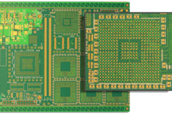
The PCB board is composed of multiple layers, PCB classification by layer refers to the number of layers of electrical layers. However, the non-electrical layer is basically what every PCB has, understanding the purpose and meaning of each layers helps us better design PCBs.
Table of Contents
Silkscreen Layers
Generally, the white characters and wire frame on the PCB is the silkscreen layer (if the solder mask of the board is white, the silkscreen is black), which is used to mark the designator, component frame and some remarks.
SolderMask Layers
Generally, the green on the surface of the PCB board is the soldermask layer (of course there are other colors, the more commonly used are blue, black, white, red, yellow, but green is used by default), which plays an insulating role. Note: this layer is a negative film, which means that there is no green where there is a drawing, and there is green where there is no drawing.
PasteMask Layers
The pastemask layer is also known as a paste layer or a stencil layer. Generally, a layer of tin or gold plating on the pads of the PCB board is the pastemask layer, which is used to assist soldering and make soldering easier. In the design, this layer is a positive film.
Mechanical Layers
The mechanical layer is designed to carry out some physical and mechanical properties, such as borders, slots, openings, and so on. Generally, there can be multiple mechanical layers, the role of the layer can be customized, and dimensioning can also be performed. There will be differences between different software.
Assembly Layers
The assembly layer is generally used in PCBA processing to mark the position and direction of component assembly. Of course, this layer can also be replaced by a silkscreen layer. This layer is no longer displayed on the physical PCB, but can be printed out for staff viewing.
Keep-Out layer
The Keep-Out layer is mainly used for constraints. For example, there are places where copper is not allowed or traces and vias are not allowed. This area can be marked on the Keep-Out layer.
Drill Layer
The drill layer contains drill data such as vias, via pads, etc.
Electrical Layers
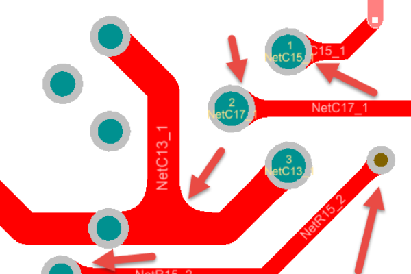
The electrical layer includes the top layer, the middle layer (multi-layer board) and the bottom layer, which have electrical connection properties. Most of the design work is to design this layer. Conduct reasonable wiring on the electrical layer, and connect the pins of the component package reasonably. Copper plating is also done on the electrical layer.
Substrate
The substrate is the insulating medium layer between the electrical layers, commonly used are FR-4 epoxy glass fiber, of course, there are aluminum substrates, flexible boards and so on. Choose the appropriate substrate according to the specific application.
The above is the introduction of the use of each layer of the PCB. If you have any questions or suggestions, you can leave a message to us.