Table of Contents
Executive Summary
Teardrops represent a critical yet often overlooked aspect of PCB design that significantly impacts manufacturing reliability, mechanical stability, and signal integrity. These tapered transitions between traces and pads/ vias serve multiple functions—from preventing trace separation during drilling operations to improving impedance continuity in high-speed circuits. This comprehensive guide explores the engineering rationale behind teardrop implementation, examines different application scenarios, analyzes potential trade-offs, and provides practical implementation guidelines for PCB designers across consumer electronics, automotive systems, and high-reliability industrial applications.
1.Understanding Teardrops: Fundamental Concepts
1.1 What Are Teardrops?
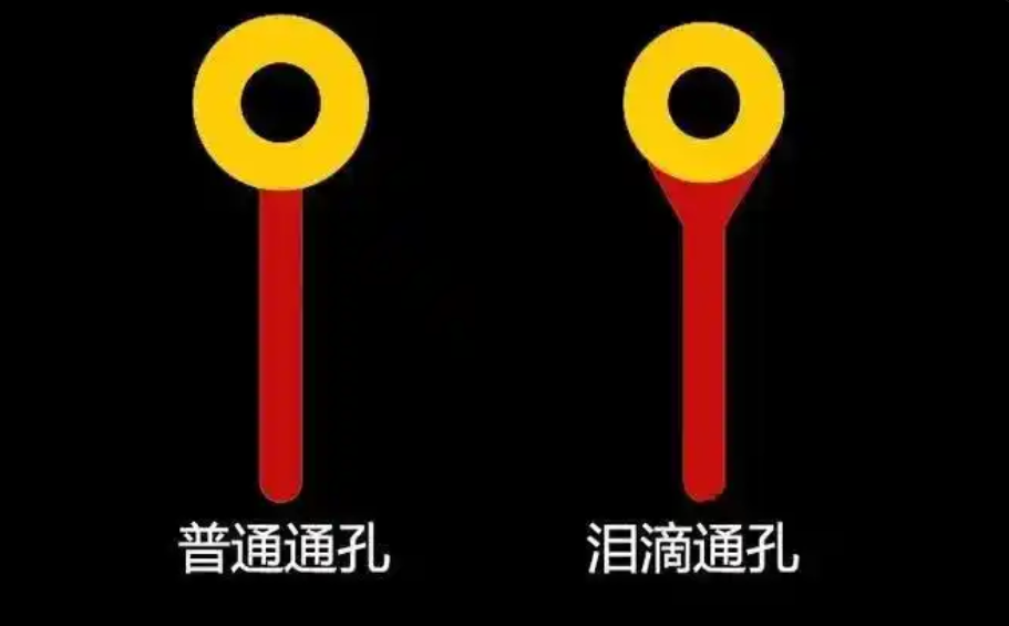
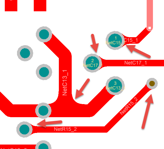
In PCB design, teardrops refer to the tapered, tear-shaped transitions between conductive traces and their termination points at pads or vias . This design feature expands the connection area at these critical junctions, creating a more robust interface between different PCB elements. The teardrop shape typically features a gradual width transition that follows either a linear or curved profile, depending on the specific design requirements and manufacturing capabilities.
The terminology varies slightly between different design contexts—while digital and general PCB designers refer to them as “teardrops,” RF and microwave engineers typically use the term “tapered transitions” to describe similar structures . Despite the naming difference, the fundamental purpose remains consistent: to create a more reliable connection at impedance-critical or mechanically vulnerable points in the circuit layout.
1.2 Historical Context and Evolution
The implementation of teardrops in PCB design has evolved significantly alongside manufacturing technologies and application requirements. Initially, teardrops were primarily employed as a reliability enhancement feature for PCBs produced with less precise drilling equipment, where drill wander could easily sever connections to pads and vias . As electronic devices progressed toward higher frequencies and smaller form factors, the functional scope of teardrops expanded to address impedance continuity and thermal management challenges in advanced applications.
Modern EDA tools have dramatically simplified teardrop implementation, with platforms like Jialichuan EDA Professional Edition incorporating dedicated teardrop tools that support both trace-to-pad and T-shaped connections with edges for improved aesthetics and performance . This evolution has transformed teardrops from a manual design technique to an automated feature accessible to designers across experience levels.
2.Key Benefits and Functional Advantages
2.1 Enhanced Mechanical Reliability
The primary advantage of teardrop implementation lies in significantly improved mechanical robustness at connection points:
•Drilling Stress Mitigation: During PCB fabrication, drilling operations—particularly for vias—subject the board to substantial mechanical stress. Teardrops reinforce these vulnerable points, preventing connection failure when drill bits slightly miss their targets . Jiepei’s manufacturing data indicates that teardrops can compensate for layer-to-layer misalignment up to 0.05mm, substantially reducing the risk of “broken holes” .
•Vibration and Impact Resistance: In applications exposed to mechanical vibration or potential impact—such as automotive electronics and industrial controllers—teardrops distribute external forces across a larger connection area. This reinforcement increases resistance to trace separation by 40-60% in connector regions where mechanical stress is concentrated .
•Thermal Stress Management: During soldering operations and thermal cycling, different PCB materials expand at varying rates. Teardrops with approximately 0.2mm transition zones can reduce stress caused by thermal expansion mismatches by up to 35%, preventing pad lifting and connection fractures .
2.2 Manufacturing and Assembly Improvements
Teardrops deliver substantial benefits throughout the manufacturing and assembly process:
•Production Yield Enhancement: According to statistical data from Jiepei PCB, implementing teardrops in HDI boards improves production yield by 3-5% by compensating for various manufacturing imperfections .
•Soldering Reliability: The expanded connection area provides additional protection against pad lifting during multiple soldering/desoldering cycles, particularly valuable for components requiring frequent replacement or repair .
•Etching Process Optimization: Teardrops facilitate more uniform copper etching during PCB fabrication, preventing acid traps and ensuring cleaner copper surfaces without residual etchants .
2.3 Signal Integrity Considerations
Properly implemented teardrops can positively impact electrical performance in specific scenarios:
•Impedance Smoothing: When correctly designed, teardrops create a gradual impedance transition at connections, reducing reflections caused by abrupt width changes . In the 1-3GHz frequency range, appropriately shaped弧形 teardrops can reduce impedance fluctuations by approximately 15% .
•Reduced Reflection: The tapered transition minimizes the impedance discontinuity that occurs when signals move between traces and pads, particularly beneficial for higher-speed digital interfaces .
Table: Teardrop Impact Analysis Across Frequency Ranges
| Frequency Range | Impedance Stability | Recommended Approach |
| < 1 GHz | Minimal impact | Standard teardrop implementation |
| 1-3 GHz | 15% improvement with optimal design | 弧形 teardrops with controlled taper |
| 3-5 GHz | Potential degradation if poorly designed | Simulation-verified profiles |
| > 5 GHz | Risk of 0.5dB insertion loss | Avoid or use minimal transitions |
3.Teardrop Implementation Guidelines
3.1 Critical Application Scenarios
Certain PCB configurations particularly benefit from teardrop implementation:
•High-Stress Mechanical Areas: Components subject to physical connection/disconnection cycles or mechanical vibration—including connectors, large-current terminals, and motor drive boards—require teardrops for reinforced connections .
•High-Reliability Domains: Applications with stringent reliability requirements, such as automotive electronics, aerospace systems, and medical devices, often implement teardrops per IPC Class 3 standards or other industry-specific requirements .
•BGA Escape Routing: For 0.5mm pitch BGA devices, micro-teardrops with extension amounts ≤0.05mm enhance connection reliability without compromising routing density .
•Frequently Repaired Areas: Test points and components requiring regular replacement or rework benefit from teardrops that prevent trace damage during maintenance operations .
3.2 Selective Implementation Scenarios
Some applications warrant careful evaluation before teardrop implementation:
•Power Filtering Capacitors: In multi-layer boards, gradient teardrops at internal layer connections can alleviate thermal deformation stress .
•Low-Speed Signal Traces: For traces wider than 20mil, teardrops may be unnecessary but can still provide benefits at via connections .
•Cost-Sensitive Consumer Electronics: Implementation should be balanced against manufacturer capabilities, with teardrop sizes potentially increased when drilling precision is lower .
3.3 Contraindicated Scenarios
Specific applications may be better served without teardrops:
•High-Frequency/Millimeter-Wave Circuits: Antenna feed points and 24GHz radar modules often maintain better impedance continuity without teardrops, which can disrupt carefully tuned transmission line structures .
•High-Density BGA Breakout Regions: For 0.4mm pitch BGA devices, available routing space takes priority over teardrop implementation .
•Flexible Circuits: Standard right-angle teardrops should be avoided in bend areas, with elliptical transition structures preferred when reinforcement is necessary .
4.Technical Considerations and Potential Drawbacks
4.1 Signal Integrity Implications
While teardrops offer mechanical benefits, they introduce potential signal integrity challenges, particularly in high-speed designs:
•Impedance Discontinuities: Contrary to conventional wisdom, teardrops often worsen impedance matching rather than improving it . Both narrow pads connecting to wider traces and wide pads connecting to narrower traces typically show degraded return loss with longer taper lengths .
•High-Frequency Limitations: As digital signal speeds increase into the multi-gigabit range, teardrops can introduce impedance variations that negatively impact signal quality. For differential pairs specifically, teardrops effectively create coupled tapers whose properties depend on trace spacing, taper rate, and profile .
•Bandwidth Constraints: From an RF perspective, teardrop tapers behave like high-pass filters with specific electrical lengths. As taper sizes decrease, bandwidth limitations extend to higher frequencies, but this may still fall within the operating range of modern high-speed interfaces .
4.2 Layout and Density Challenges
Teardrop implementation presents specific physical design constraints:
•Space Allocation: In high-density designs such as smartphone motherboards, teardrop width should generally not exceed 1.5 times the trace width (e.g., 0.15mm teardrops for 0.1mm traces) to prevent obstruction of adjacent routing channels .
•Differential Pair Considerations: Maintaining consistent edge-to-edge spacing through tapered sections is crucial for differential pairs. Angling teardrops to preserve this spacing helps minimize impedance deviations .
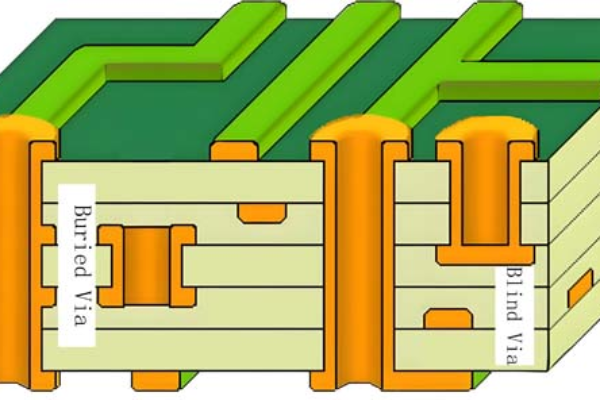
•Manufacturing Precision: HDI boards require laser-cut micro-teardrops with precision up to ±0.01mm, while thick copper boards need compensation factors (copper thickness/3) to prevent uneven etching .
5.Design Implementation Guidelines
5.1 Optimal Teardrop Parameters
Successful teardrop implementation requires careful parameter selection:
•Taper Length Selection: For applications with wider signal bandwidths, shorter taper distances are generally preferable to minimize high-frequency disruptions .
•Profile Optimization:弧形 teardrop profiles typically provide superior performance to linear tapers, offering smoother impedance transitions and reduced reflection .
•Spacing Management: For differential pairs, maintaining consistent edge-to-edge spacing through tapered sections helps control impedance variations .
5.2 Process-Specific Recommendations
Different manufacturing processes require tailored teardrop approaches:
•HDI Boards: Laser-cut micro-teardrops with ±0.01mm precision ensure optimal results in high-density applications .
•Thick Copper Boards: Implementing teardrop compensation factors (copper thickness/3) prevents etching irregularities .
•Rigid-Flex Boards:弧形 transitions in bending areas prevent stress concentration and potential fracture points .
5.3 Verification Methodologies
Robust teardrop implementation requires appropriate validation techniques:
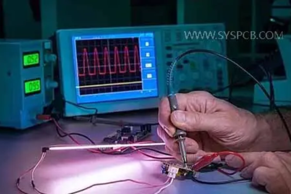
•Impedance Testing: For RF lines and differential pairs, vector network analyzer testing of S-parameters verifies impedance stability after teardrop application .
•Simulation Analysis: Specialized electromagnetic solvers (HFSS, SIwave, Simbeor) can semi-automatically calculate S-parameters, particularly S11 (return loss), to identify unacceptable impedance deviations when teardrops are applied to traces .
•Visual Inspection: Ensuring proper teardrop formation without manufacturing defects such as incomplete copper coverage or residual etching contaminants .
6.Future Trends and Industry Outlook
6.1 Technology Evolution
Teardrop implementation continues to evolve alongside PCB technology trends:
•Automated Optimization: Advanced EDA tools increasingly incorporate automated teardrop features that balance mechanical requirements with signal integrity considerations .
•Application-Specific Profiles: Growing recognition that different scenarios require customized teardrop approaches rather than one-size-fits-all implementations .
•High-Frequency Adaptations: As digital speeds increase, teardrop strategies must adapt to maintain signal integrity while providing mechanical benefits .
6.2 Manufacturing Advancements
Emerging manufacturing capabilities enable more sophisticated teardrop applications:
•Precision Fabrication: Improved drilling and etching technologies allow for smaller, more precise teardrops that minimize spatial impact while providing reinforcement benefits .
•Material Compatibility: Advanced substrate materials require tailored teardrop approaches to address unique thermal and mechanical characteristics .
•Quality Verification: Enhanced inspection methodologies provide better feedback on teardrop implementation effectiveness, driving continuous improvement .
7.Conclusion
Teardrop implementation represents a nuanced aspect of PCB design that requires careful consideration of mechanical, manufacturing, and electrical factors. While offering significant benefits for mechanical reliability, production yield, and assembly durability, teardrops introduce potential signal integrity challenges that must be carefully managed, particularly in high-speed applications.
The decision to implement teardrops should be based on specific application requirements rather than universal rules. Mechanical stress concerns, manufacturing capabilities, and signal frequency content all influence the optimal approach. By understanding the trade-offs involved and following implementation best practices, PCB designers can effectively leverage teardrops to enhance product reliability without compromising performance.
As PCB technology continues advancing toward higher frequencies, greater densities, and more diverse applications, teardrop implementation strategies will likewise evolve, requiring ongoing attention to both established principles and emerging developments in the field.
Partner with Us for Your PCB Manufacturing Needs
Our expertise in advanced PCB manufacturing and design optimization ensures that your teardrop implementation strategies are effectively translated into reliable, high-performance physical boards. With specialized capabilities in HDI technology, impedance control, and rigorous quality assurance, we deliver solutions that balance mechanical robustness with signal integrity requirements.
Contact us today to discuss how we can support your next PCB project with manufacturing expertise tailored to your specific application requirements and reliability targets.