Rigorous testing protocols prevent up to 98% of field failures in electronic assemblies. As PCB complexity increases with 01005 components and 0.3mm-pitch BGAs, advanced testing strategies have become non-negotiable for mission-critical applications. This guide examines cutting-edge testing methodologies across every assembly stage.
Table of Contents
1. Solder Paste Printing Stage: The First Line of Defense
3D Solder Paste Inspection (SPI)
– Technology: Laser profilometry + moiré interferometry
– Key Metrics:
– Height accuracy: ±5μm
– Area coverage: >99.5%
– Volume tolerance: ±10%
– Industry Standard: IPC-7527 (Acceptance Criteria 90-110% volume)
Critical Process Controls
| Parameter | Optimal Range | Defect Prevention |
| Stencil Alignment | ±25μm | Prevents bridging |
| Paste Viscosity | 800-1,200 kcps | Avoids slump and cold joints |
| Squeegee Pressure | 0.3-0.5 kg/cm | Eliminates smearing |
> Case Study: Implementing real-time SPI reduced solder defects by 73% at Foxconn’s IoT production line.
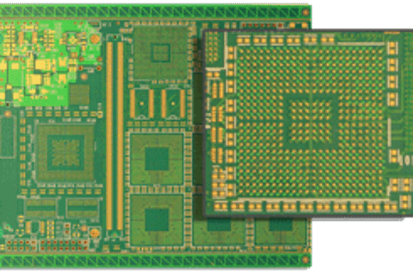
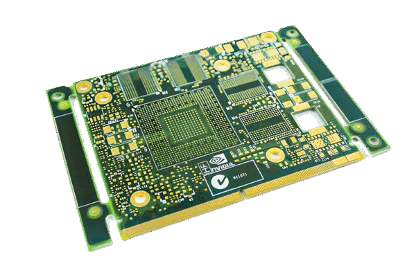
2. Component Placement Verification
Machine Vision Alignment
– Precision: ±15μm @ 3σ (for 01005 components)
– Algorithms: Pattern matching + CAD comparison
Placement Accuracy Testing
– Laser Calibration: Verifies nozzle positioning accuracy every 4 hours
– First Article Inspection: Measures 100% component positions with 5μm-resolution cameras
– Acceptance Criteria: IPC-A-610 Class 3 – 50% pad contact minimum
3. Reflow Soldering Validation
Thermal Profiling

– Monitoring Tools:
– K-type thermocouples with 0.5°C accuracy
– Real-time O₂ sensors (<1000ppm for nitrogen reflow)
Post-Reflow Inspection
– Automated Optical Inspection (AOI):
– Detects tombstoning, skew, and bridging
– 10MP cameras resolve 15μm defects
– X-ray Inspection (AXI):
– 5μm resolution for BGA voids (IPC-7095: <25% void area)
4. Electrical Performance Testing
In-Circuit Test (ICT)
– Fixturing: 10,000+ probe points with <20mΩ contact resistance
– Key Checks:
– Shorts/opens detection
– Component value verification (±2% tolerance)
– Power-on functional test
Flying Probe Test
– Advantages: No fixture cost, 100μm probe positioning
– Throughput: 30-50 tests/minute vs ICT’s 500+/minute
5. Functional & System-Level Validation
Boundary Scan (JTAG IEEE 1149.1)
– Tests interconnects on unpopulated boards
– Coverage: >85% of digital nets
Environmental Stress Screening (ESS)
| Test Type | Parameters | Duration |
| Thermal Cycling | -40°C ↔ +85°C, 10 cycles | 48 hours |
| Vibration | 5-500Hz, 5Grms | 1 hour/axis |
| Burn-in | 125°C, 100% load | 24-168 hours |
6. Reliability & Lifetime Validation
Accelerated Life Testing
– Arrhenius Model:
| AF = e^[(Ea/k)(1/T_use – 1/T_test)] |
(Ea=0.7eV for consumer electronics)
– Example: 500 hours @ 85°C/85%RH = 5 years field life
Failure Analysis Tools
– SEM-EDS: Identifies intermetallic compound (IMC) failures
– Cross-Sectioning: Measures solder joint integrity per IPC-J-STD-001
7. Emerging Test Technologies
AI-Powered Quality Systems
– Predictive Analytics:
Machine learning correlates SPI/AOI data to predict solder joint reliability (92% accuracy)
– Generative Adversarial Networks:
Create synthetic defect images to train inspection algorithms
Industrial IoT Integration
– Real-Time Monitoring:
Edge computing analyzes 10,000+ test parameters/second
– Blockchain Traceability:
Encrypted test records for automotive/medical compliance
Testing Strategy ROI Analysis
| Technology | Upfront Cost | Defect Reduction | ROI Period |
| 3D SPI | $120,000 | 40-60% | 14 months |
| AXI | $350,000 | 80-92% | 22 months |
| JTAG/Boundary | $75,000 | 30-45% | 8 months |
→ [Download PCB Test Strategy Planner]
Includes: IPC compliance checklists, cost-benefit models, AI implementation guide