Table of Contents
The Wi-Fi 7 Transformation: Beyond Speed
Wi-Fi 7 (IEEE 802.11be) marks a paradigm shift in wireless technology, delivering unprecedented 80 Gbps speeds, sub-2ms latency, and multi-device reliability—enabling applications from industrial automation to immersive XR. Unlike incremental upgrades, its core innovations demand radical changes in PCB design and manufacturing:
– 4096-QAM modulation boosts data density by 20% vs. Wi-Fi 6’s 1024-QAM, requiring ultra-precise impedance control to preserve signal integrity.
– 320 MHz channel bandwidth (double Wi-Fi 6’s 160 MHz) necessitates low-loss laminates to minimize dielectric attenuation at 6 GHz frequencies.
– Multi-Link Operation (MLO) enables simultaneous 2.4/5/6 GHz band aggregation, demanding complex RF isolation on PCBs to prevent crosstalk.
The global adoption surge is undeniable: enterprises deploying Wi-Fi7 report 40% higher multi-device concurrency and 90% lower latency in manufacturing automation and AR classrooms.
PCB Design Challenges: Where Wi-Fi 7 Demands Perfection
1. Signal Integrity at 6 GHz and Beyond
Wi-Fi7’s shift to 6 GHz bands amplifies high-frequency losses:
– Impedance Control: 85 Ω differential pairs require ±5% tolerance—deviations distort 4096-QAM constellations.
– Material Selection: Low-Dk/Df laminates like Rogers 4350B or Megtron 6 (Df ≤0.003) are essential to maintain <0.1 dB/mm loss at 14 GHz.
– Via Optimization: Stub lengths >200 mils cause reflections—laser-drilled microvias and via-in-pad are mandatory for 0.4mm-pitch SoCs like the IPQ9574.
2. Thermal Management for High-Power SoCs
Wi-Fi7 SoCs (e.g., MediaTek Filogic 660) generate 15–25W heat loads during 320 MHz operation:
– Copper Coin Embedding: Direct-bonded Cu slugs under BGA packages reduce θJA by 60% vs. standard thermal vias.
– High-Tg Substrates: Materials with Tg ≥170°C withstand repeated reflow cycles without delamination.
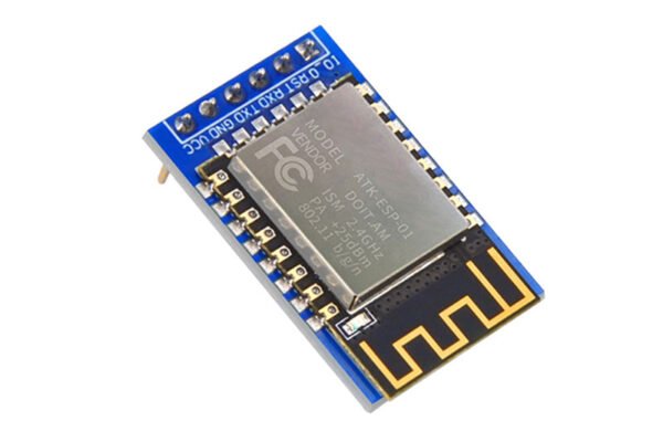
3. Multi-Antenna System Integration
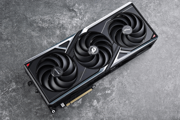
Advanced routers like the 18-antenna BE7200 CPE require:
– Cross-Band Isolation: Separate PCB zones for 2.4/5/6 GHz antennas with grounded guard rings.
– Shielded Cavities: Multi-chamber EMI shields prevent noise coupling between cellular (5G) and Wi-Fi radios.
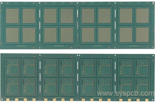
Material & Manufacturing Breakthroughs for Wi-Fi 7 Success
Table: Critical PCB Technologies for Wi-Fi 7 Applications
| Requirement | PCB Solution | Performance Gain |
| 6 GHz Signal Loss | Ultra-Low Loss Rogers 4350B | 50% lower attenuation vs. FR-4 |
| SoC Thermal Density | Embedded Cu Coins + AlN Patches | 15W/cm² dissipation, no heatsink |
| High-Density Routing | Any-Layer HDI (30/30μm L/S) | 0.3mm BGA escape routing |
| EMI Control | Laser-Cut Shield Walls | 30 dB crosstalk suppression |
| Miniaturization | 01005 Components + SiP Modules | 60% size reduction for Wi-Fi 7 APs |
Real-World Applications Driving PCB Innovation
1.Enterprise Access Points
–12+ Layer HDI Boards: Support 16-stream MU-MIMO via dense SoC fanouts (e.g., Qualcomm IPQ9574).
–Dynamic Frequency Selection (DFS) Antennas: Dedicated RF tracks with 50 Ω impedance for interference avoidance.
2.Consumer Routers & CPEs
–Rigid-Flex Designs: Enable compact folding in Wi-Fi 7 mesh nodes.
–Multi-PCB Stacking: Isolate noise-sensitive GNSS/DFS antennas from high-power transceivers.
3.Industrial IoT Gateways
–Metal-Core PCBs: Dissipate heat in machine vision systems requiring 24/7 reliability.
–Conformal Coatings: Protect against humidity/chemicals in factories.
The Manufacturing Imperative: Precision Meets Scalability
Wi-Fi 7 PCBs demand semiconductor-grade fabrication:
– Impedance Testing: TDR validation with 85 Ω fixtures (not standard 50 Ω).
– Plating Uniformity: ≤10% Cu thickness variation in microvias to prevent current hotspots.
– AOI/X-Ray: 100% inspection of 0.4mm-pitch solder joints.
Failure Risks in Mass Production:
> “Substituting uncertified MOSFETs or laminates caused 23% of early Wi-Fi 7 failures during thermal stress testing.” — IPCB Labs Report
Why Partner with SysPCB?
We enable cutting-edge Wi-Fi 7 products through:
– 6 GHz-Optimized Stackups: Pre-validated layer configurations with Rogers/Megtron laminates.
– Thermal Superhighways: Cu coin embedding + high-thermal-conductivity dielectrics.
–Any-Layer mSAP: 30/30μm trace/space for 0.3mm CSP fanouts.
–EMI/RF Expertise: Cavity shielding and antenna isolation techniques.
Proven Results:
– 70% reduction in multi-antenna crosstalk for 18-antenna CPEs
– 0.1 dB insertion loss at 14 GHz for 320 MHz channels
The Future: AI, 6G, and Beyond
Wi-Fi 8 (802.11bn) will push frequencies beyond 10 GHz, demanding:
– D-Band RF PCBs: 140 GHz-ready PTFE composites.
– Embedded AI Accelerators: On-PCB inference chips for predictive network optimization.
– Sustainable Materials: Halogen-free, high-recycle-content substrates aligning with ESG goals.
“In the Wi-Fi 7 era, your PCB isn’t just a carrier—it’s the foundation of performance. At 6 GHz, every micron of copper and every laminate choice defines success.”
Ready to Design Winning Wi-Fi 7 Hardware?
→ [Download Our Wi-Fi 7 Stackup Design Kit]
→ [Request a Signal Integrity Audit]
→ [Explore Certified Manufacturing Options]