Table of Contents
The USB4 Transformation
USB4 represents a quantum leap in connectivity, delivering 80 Gbps speeds (USB4 v2), dynamic bandwidth allocation, and multi-protocol support—all through the versatile USB Type-C interface. As the first USB standard built on Intel’s Thunderbolt protocol, it unifies data, video, and power delivery while maintaining backward compatibility with USB 3.2/2.0 and Thunderbolt 3. For PCB designers and manufacturers, this revolution demands unprecedented precision in signal integrity, thermal management, and material innovation.
USB4 Technical Specifications: Beyond Speed
Table: USB4 Generations Compared
| Parameter | USB4 Gen 1 | USB4 Gen 2 | USB4 v2 (Gen 4) |
| Max Speed | 20 Gbps | 40 Gbps | 80 Gbps |
| Signaling | NRZ | NRZ | PAM3 |
| Modulation | 2-level | 2-level | 3-level |
| Key Applications | Laptops, Docks | External GPUs | 8K VR, AI Clusters |
| Backward Compat | USB 3.2/2.0 | Thunderbolt 3 | Thunderbolt 4/5 |
Core Innovations Driving Performance:
1.Dual-Lane Architecture:
Leverages existing USB-C cables with dual-channel operation to achieve 40 Gbps (Gen 2) and 80 Gbps (Gen 4) speeds.
2.Protocol Agnosticism:
Dynamically shares bandwidth between data (USB, PCIe) and display protocols (DisplayPort 2.1), enabling simultaneous 8K video streaming and 5 GB/s file transfers.
3.Thunderbolt Integration:
Inherits Intel’s Thunderbolt 3 spec—allowing daisy-chaining GPUs, displays, and storage without licensing fees.
Critical PCB Design Challenges for USB4 Systems
Signal Integrity at 80 Gbps
USB4 v2’s PAM3 modulation triples data density but amplifies sensitivity to noise and loss:
– Impedance Control: Requires 85 Ω differential pairs (tolerance ≤±5%) and 42.5 Ω single-ended reference—deviations cause reflections degrading PAM3 eye diagrams.
– Loss Budget: At 14 GHz Nyquist frequency (Gen 4), dielectric losses dominate:
Total Channel Loss = Conductor Loss + Dielectric Loss + Reflection Loss
Solutions: Low-Dk/Df laminates (Rogers 4350B, Megtron 6) with ≤0.003 loss tangent.
– Stub Elimination: Vias/stubs >200 mils create impedance discontinuities—use microvias and laser-drilled pads for BGA escapes.

Thermal & Power Integrity
•Current Density: 100W power delivery (20V/5A) demands 2 oz copper planes with thermal relief under connectors.
•Via Optimization: Staggered thermal vias (aspect ratio ≤8:1) under controllers reduce θJA by 40% vs. clustered vias.
EMI Mitigation
PAM3’s wider spectrum increases EMI risk:
– Guard Traces: 30-μm gaps with grounded stitching vias isolate differential pairs.
– Shielding: Full-ground layers between signal strata absorb crosstalk.
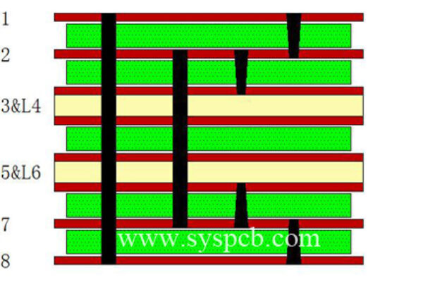
Advanced Materials & Stackups for USB4 Success
Layer Stackup Recommendations
| Layer | Material | Function |
| L1 | Rogers 4350B (3.5 mil) | High-speed USB4 pairs |
| L2 | FR-4 (2 oz Cu) | Ground plane (continuous) |
| L3 | Megtron 6 (4 mil) | PCIe/DisplayPort lanes |
| L4 | FR-4 (1 oz Cu) | Power delivery + low-speed signals |
Note: Total thickness ≤0.8mm for 16-layer designs
Material Selection Criteria:
– Dk Consistency: ±0.05 variation across panels (critical for PAM3 timing)
– Thermal Stability: Tg ≥170°C to survive reflow cycles
– CAF Resistance: ≥100MΩ at 85°C/85% RH per IPC-650
Manufacturing Imperatives for USB4 Compliance
1.Impedance Validation:
TDR testing with 42.5 Ω fixtures—not standard 50 Ω—to match USB4 spec.
2.Plating Uniformity:
Copper thickness variation ≤10% in microvias to prevent current crowding.
3.Surface Finishes:
ENIG or Immersion Silver for ≤0.3μm roughness (reduces skin effect losses).
Critical Tests for Signal Integrity:
– Return Loss: ≤-8.5 dB up to 14 GHz for Gen 4
– Integrated Return Loss (IRL): ≤-14.5 dB for RX, ≤-15 dB + margin for TX
– ISI Margin: Validated via PRTS7/PRBS31 patterns with VNA/S-parameter analysis
Real-World Applications Demanding USB4 PCBs
•8K VR Headsets: 16-layer HDI with embedded optical engines (≤30μm line/space)
•AI Accelerator Docks: 10-layer rigid-flex designs with 0.3mm pitch CSPs
•Medical Imaging Systems: Any-layer HDI for 40 Gbps ultrasound data pipelines
Why Partner with SysPCB?
We enable robust USB4 implementations through:
Impedance Control: ±3% tolerance on 85 Ω diff pairs via field-solving EM tools
Thermal Superhighways: Embedded copper coins + AlN substrates for 15W/cm² dissipation
Certification Support: Pre-compliance testing with USB-IF approved methodologies
High-Density Expertise: 30/30μm trace/space for 0.4mm BGA fanouts
Design Guidelines We Enforce:
– No 90° turns: Two 45° arcs or curves only
– Length matching: ≤0.1mm skew for MIPI-CSI2/USB4 pairs
– Plane avoidance: Keep-out zones under crystals/oscillators
“USB4 isn’t just faster USB—it’s a convergence of data, display, and power that demands PCBs behave like precision RF systems. At 80 Gbps, your substrate is the signal.”
Ready to Build Future-Ready USB4 Systems?
→ [Download Our USB4 Stackup Design Kit]
→ [Request Signal Integrity Pre-Check]
→ [Explore Certified Manufacturing Options]