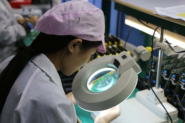
DIP processing technology, also known as “through-hole”, refers to an installation scheme for electronic components, by manual assembly (manual placement) or by using an automatic plug-in mounting machine, insert the components in to the drill holes and solder them to the pads on the PCB.
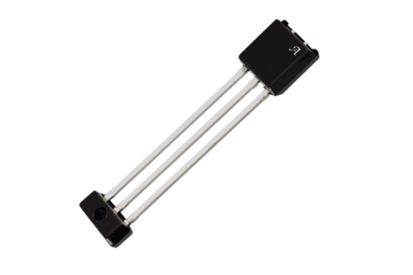
DIP components
First, the advantages of DIP processing
1, DIP processing provides a strong mechanical combination, more robust than SMT technology, suitable for aerospace and other fields with high robustness.
2. Prototyping engineers generally prefer larger through holes rather than surface mount components because they can be easily used with board sockets.
Second, the disadvantages of DIP processing
1. Although DIP processing provides a strong mechanical combination compared to SMT technology, but need additional drilling, this make the PCB bare board more expensive.
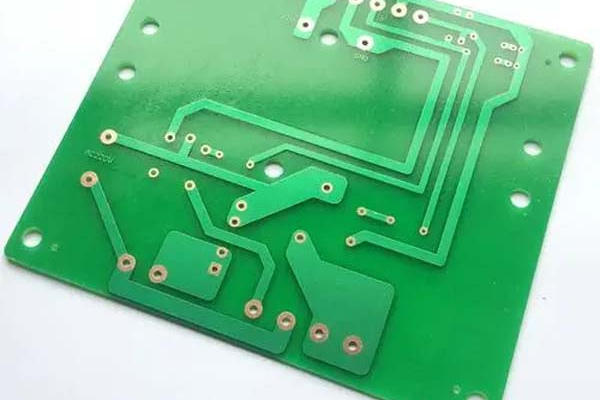
2. They also limit the available wiring area in the multilayer board because the holes must pass through all layers to the opposite side. To this end, DIP techniques are now generally reserved for larger or heavier components, such as larger packaged electrolytic capacitors or semiconductors, such as TO220 that require additional mounting strength, or require powerful components such as plug connectors or electromechanical relays.
3. However, high speed or high frequency designs may require SMT technology to minimize the stray inductance and capacitance in the wires, thereby damaging the circuit function. Even in the prototype phase of the design, ultra-small designs may require an SMT structure.