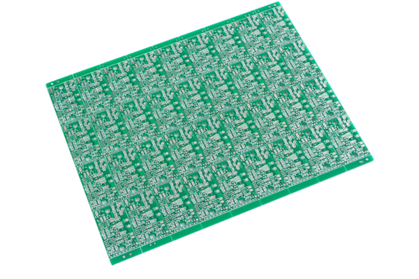
In the field of PCB manufacturing, over 85% of multi-layer boards adopt even layer designs, which is not accidental but a comprehensive decision based on core process principles and cost-effectiveness. The following is a technical analysis of the key reasons:
Table of Contents
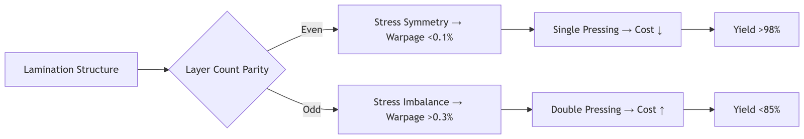
1、 Structural stability: a necessary requirement for thermodynamic symmetry
1. Laminated stress balance
During PCB lamination, there is a significant difference in the coefficient of expansion between the copper layer (CTE ≈ 17ppm/° C) and the resin layer (CTE ≈ 60ppm/° C) at high temperatures. Even numbered layers achieve stress cancellation through mirror symmetric structures (such as 6-layer board: L1-L2-Core-L3-L4-PP-L5-L6), controlling the thermal deformation to ≤ 0.1mm/m (IPC-6012 standard).
Odd layer problem: Asymmetric structure leads to stress concentration in the Z-axis, and the warpage rate increases by 3-5 times after reflow soldering.
2. Uniformity of medium thickness
The semi cured sheet (Prepreg) of even numbered laminates is symmetrically distributed (such as 8-layer laminates with consistent PP thickness between 2-3/4-5/6-7 layers), and the signal impedance fluctuation is less than ± 5%.
Odd layer case: A 7-layer board requires the addition of PP on one side of the core layer, resulting in a deviation of L3-L4 dielectric thickness ≥ 15% and impedance control failure.
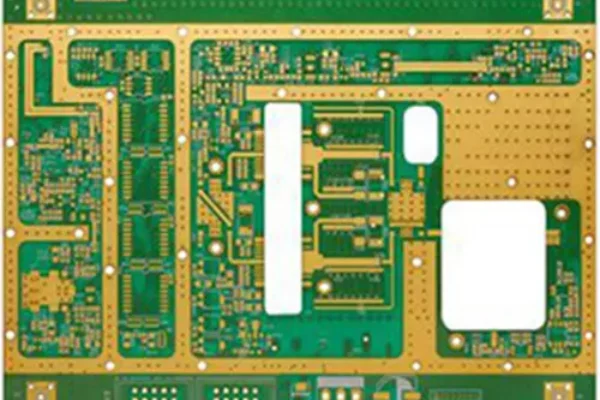
2、 Cost Efficiency: Optimization Rules for Materials and Processes
1. Comparison of material utilization rates (taking 6-layer vs 7-layer as an example)
| Parameters | 6-layer board | 7-layer board |
| Copper foil usage | 4 sheets (inner layer 2+outer layer 2) | 5 sheets (additional 1 copper foil required) |
| Semi cured film | 3 sheets (symmetrical distribution) | 4 sheets (asymmetrical stacking) |
| Yield loss | benchmark value | increase by 12-18% (due to warping) |
| Single piece cost increase | – | +23-30% |
2. Simplification of processing procedures
The even layer board adopts a one-time compression (such as 1+4+1 structure), while the odd layer board requires a second compression:
-First press the core board (such as 3-layer core: L2 Core-L3)
-Adding PP and copper foil for secondary lamination on the outer layer
This process extends the production cycle by 40% and increases energy consumption by 35%.
3、 Technical Compromise Solution: The Cost of Pseudo Odd Layer Design
When odd layers are unavoidable (such as impedance layer constraints), engineers use two methods:
1. Blank signal layer method
Adding a non functional copper layer (Dummy Layer) to the core board resulted in:
-Plate thickness increased by 10%
-The interlayer capacitance deviation reaches 20%
-The cost is still higher than the equivalent even layer board (+18%)
2. Asymmetric stacking method
Directly adopting an asymmetric structure (such as 7-layer: L1-PP-L2-Core-L3-PP-L4-PP-L5-PP-L6-PP-L7), but facing:
-Reflow soldering warpage ≥ 0.3% (exceeding the 0.75% upper limit of IPC Class 3)
-High speed signal Skew increases by 15ps/inch
>Actual test data: A certain communication device uses a 9-layer board, and after thermal cycling testing (-55 ℃~125 ℃), the occurrence rate of microcracks is 6 times higher than that of an 8-layer board.
4、 Breakthrough in Advanced Technology: Alternative Solution for Odd Layer Requirements
Modern technology has weakened the reliance on odd layers:
1. Any layer interconnect (Any layer HDI)
By using laser micro hole stacking (such as 1+N+1 structure) to achieve high-density wiring, traditional 14 layer board functions can be completed within 12 layers, reducing the number of layers required.
2. Impedance compensation technology
Adopting trapezoidal cross-section routing or differential coplanar waveguide, ± 3% impedance control is achieved in even layers, replacing special impedance layers in odd layers.
3. Buried capacitance/buried resistance materials
Integrating Passive components (such as 3M C-Ply) between layers saves dedicated signal layers, and 6-layer boards can replace traditional 7-layer designs.
5、 Industry best practice: When must odd layers be used?
Only two types of scenarios require breaking through even layer limitations:
1. Ultra high voltage isolation design
The industrial control board needs to be equipped with 3mm insulation slots on the L3/L5 layers, which saves 22% space compared to the 6-layer structure.
2. Mixed medium high-frequency board
In the 77GHz automotive radar board, Rogers 4350B (FR-4 for other layers) needs to be inserted into the L4 layer to control phase error, with layer 5 being better than layer 6.
Conclusion: Even numbered layers are the golden balance between reliability and cost
Design suggestion:
-Prioritize the use of 4/6/8/10 layer standard stacking
-Replace the 13 layer requirement with 12 layer+Ay layer HDI
-Odd layers are only used as the ultimate means of EMC/impedance control
Get your exclusive quote immediately: fill out the form or send an email directly.As a professional PCB manufacturer , we will provide you with a quote service within 24 hours. Enjoy free DFM optimization and a 10% discount on SMT patches for your first order!