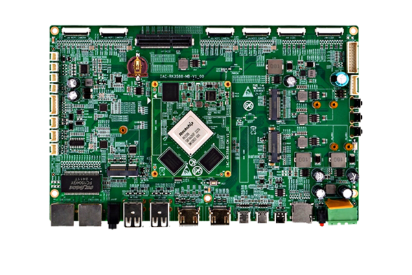
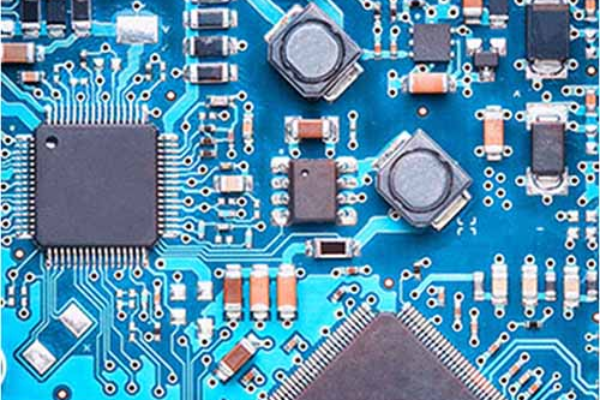
Transient Voltage Suppression (TVS) diodes are widely used in electronic circuits to protect sensitive components from voltage spikes caused by electrostatic discharge (ESD), lightning, or other transient events. While TVS diodes are critical for ensuring the longevity and reliability of electronic devices, their protection effect can be significantly influenced by the PCB (Printed Circuit Board) layout and wiring design. In this blog, we will explore how the PCB design can impact the performance of TVS diodes and how engineers can optimize their layout to maximize the protection effect.
Table of Contents
What is a TVS Diode?
A Transient Voltage Suppression (TVS) diode is a component designed to protect electronic circuits from voltage surges. It operates by clamping transient voltage to a safe level, preventing high voltage from damaging sensitive components. TVS diodes are typically used in power supplies, communication lines, and data ports, where transient events are most likely to occur.
TVS diodes can be classified into two types:
Unidirectional TVS Diodes: These protect against voltage spikes in one direction and are typically used in DC circuits.
Bidirectional TVS Diodes: These protect against voltage spikes in both directions and are commonly used in AC circuits.
Selection of TVS placement
The TVS device is as close to the noise source as possible to ensure that the surge voltage can be clamped before the pulse is coupled to the adjacent PCB wire.
Grounding options
The protection circuit should shunt the surge voltage to the case ground, if shunt the surge voltage directly to the signal ground of the integrated circuit will cause ground bounce. Reducing impedance with relatively short and wide ground leads can improve the clamping performance of TVS diodes on a single ground PCB.
Route selection
TVS wiring should avoid self-inductance. ESD is a sudden pulse of huge change, which may cause parasitic self-inductance in the loop, and then form a strong voltage shock to the loop, and may exceed the IC’s tolerance limit and cause damage. The self-inductance voltage generated by the load is proportional to the intensity of the power supply change, and the transient characteristics of ESD shocks are likely to induce high-strength self-inductance.
The basic principle of reducing parasitic self-inductance is to shorten the shunt circuit as much as possible. All factors including the ground circuit, the circuit between the TVS and the protected line, and the path from the interface to the TVS must be considered. Therefore, the TVS device should be as close as possible to the interface and as close as possible to the protected line, so as to reduce the chance of self-inductance coupling to other adjacent lines.
Loop area
Reducing the loop area formed by high-speed data and ground lines can reduce the effects of radiation and radio frequency. Especially when the wire is long, an effective way to alleviate the loop is to include a ground plate in the PCB design to increase the TVS tube to provide isolation for the separation interval between integrated circuits. But it will increase the loop area.
Other PCB Design Considerations
Apart from the aforementioned points, several other aspects of the PCB design can affect the performance of TVS diodes:
Signal Integrity: Ensure that the signal traces are properly shielded and separated from power and ground traces to reduce the likelihood of noise or transients affecting the signal.
PCB Layer Stackup: Multi-layer PCBs with dedicated ground planes can provide better noise isolation and improve the performance of TVS diodes by reducing inductive and resistive losses.
Thermal Management: TVS diodes can absorb significant amounts of energy during a transient event, and this can generate heat. Proper thermal management, including the use of heat sinks or adequate spacing around the diode, can help prevent overheating and improve the longevity of the component.
Application
In addition, the following principles can be applied to optimize the line:
1. Try to arrange the interface on the same side;
2. Avoid connecting the protected circuit and the unprotected circuit in parallel, and avoid arrange critical signal lines near the protection circuit;
3. If there are both filtering and protective circuits at the interface, the principle of protection first and filtering second should be followed. The protection circuit is used for external overvoltage and overcurrent suppression. If the protection circuit is placed after the filter circuit, the filter circuit will be damaged by overvoltage and overcurrent.
4. Keep reset, interrupt, and control signals away from the input / output ports, and away from the edges and discharge points of the PCB.
Conclusion
The protection effect of TVS diodes is closely tied to the PCB layout and wiring design. Engineers must consider the placement of the diode, trace routing, grounding, and other layout elements to ensure that the TVS diode performs at its best. By minimizing parasitic inductance, optimizing ground paths, and ensuring proper component placement, it is possible to maximize the TVS diode’s ability to protect sensitive electronics from transient voltage spikes.
A well-thought-out PCB design not only ensures the effectiveness of TVS diodes but also contributes to the overall reliability and robustness of the electronic system. Whether designing high-speed communication circuits or automotive electronics, understanding and applying best practices in PCB layout for transient voltage suppression is essential for optimal circuit protection.