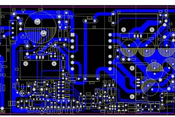
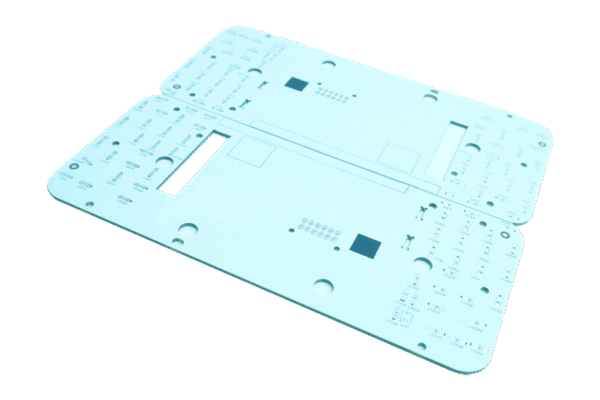
SMT Stencil is a special mold for SMT. Its main function is to help deposit the solder paste, the purpose is to transfer the exact amount of solder paste to the exact location on the empty PCB.
According to the manufacturing process of SMT stencil, it can be divided into: laser stencil, electro polishing (E.P.) stencil, electroforming (E.F.) stencil, step stencil, bonding stencil, nickel plating (Ni. P.) stencil, etching stencil.
Laser Stencil
Laser stencil is the most commonly used in the SMT stencil industry, its characteristics are:
1. Direct use of data files to reduce the production error;
2. SMT stencil opening position accuracy is extremely high: full error ≤ ± 4μm;
3. The opening of the SMT stencil has a geometric shape that facilitates the printing of the solder paste.
E.P. Stencil
The E.P. Stencil is post-treated by electrochemical means after laser cutting, its characteristics are:
1. The hole wall is smooth and is especially suitable for ultra-fine spacing such as QFP/BGA/CSP.
2. Reduce the number of wiping of SMT stencil, greatly improving work efficiency.
E.F. Stencil
In order to comply with the requirements of short, small, light and thin electronic products, ultra-fine volume (such as 0201) and ultra-dense spacing (such as BGA, CSP) are widely used, so the SMT stencil industry has also put forward higher requirements for printing stencil, electroforming stencil came into being. The electroforming stencil made by SysPCB is characterized by: Different thicknesses can be made on the same stencil.
Step Stencil
Due to the difference in the amount of solder paste required for soldering various components on the same PCB, the thickness of the same SMT stencil is required to be different, which produce the Step stencil.
Bonding Stencil
The COB components have been fixed on the PCB, but the tin-printing process is still required, which requires the bonding stencil. The Bonding stencil is to add a small cover to the PCB bonding position corresponding to the stencil to avoid the COB components.
Ni.P. Stencil
In order to reduce the friction between the solder paste and the hole wall, it is easy to demould and further improve the release effect of the solder paste.
Etching Stencil
It is made of 301 steel plate imported from the United States. The etched stencil is suitable for PCB printing with angular position and spacing greater than or equal to 0.4MM. It is suitable for use in copying board and film. It can use CAD/CAM and exposure mode at the same time, depending on different parts, it can be scaled, no need to calculate the price according to the number of parts. The production time is fast. The price is cheaper than the laser template. It is easy for customers to archive the film.