In modern electronic devices, printed circuit boards (PCBs) are like the “neural network” of electronic products, carrying the interconnection and signal transmission of electronic components. The inner layer process of PCB, as the cornerstone of the entire manufacturing process, plays a decisive role in the electrical performance, stability, and reliability of the circuit board. This article will delve into the core process, key technologies, and quality control points of PCB inner layer technology, revealing the technical secrets behind it.
Table of Contents
1、 Overview of PCB Inner Layer Process
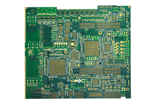
The inner layer process of PCB mainly focuses on the processing of conductive layers inside multi-layer boards. Its core goal is to accurately construct conductive circuit patterns that meet design requirements on insulating substrates, while ensuring good electrical isolation and connection between each layer. The quality of the inner layer process directly affects the smooth progress of subsequent pressing, drilling, electroplating and other processes, as well as the performance of the final product. Common PCB inner layer materials include copper-clad laminate (CCL), which is composed of copper foil and insulating substrate (such as FR-4). The thickness of copper foil is usually 18 μ m, 35 μ m and other specifications, while the insulating substrate needs to have good electrical insulation and mechanical strength.
2、 Detailed explanation of PCB inner layer process flow
(1) Cutting materials
Cutting is the first step in the inner layer process, which involves cutting large-sized copper-clad laminates into suitable small pieces based on design dimensions and production requirements. This process requires strict control of dimensional accuracy, generally allowing an error within ± 0.1mm to ensure the adaptability of subsequent processes. At the same time, attention should be paid to avoiding defects such as burrs and cracks on the edges of the board to prevent delamination and other issues during subsequent processing.
(2) Inner layer graphic transfer
Graphic transfer is a crucial step in transferring the designed circuit graphics from the negative film to the surface of the copper-clad copper foil. Firstly, cleaning treatment is carried out to remove impurities such as oxide layer and oil stains on the surface of the copper foil through chemical cleaning or mechanical polishing, enhancing the adhesion between the subsequent photoresist and the copper foil.

Then, dry film or wet film lithography technology is used to evenly coat the photoresist on the surface of the copper foil. After exposure and development, the photoresist undergoes photochemical reactions according to the pattern of the film, leaving the copper foil area that needs to be etched. In the exposure process, it is necessary to precisely control the exposure energy. Excessive or insufficient energy can cause graphic distortion and affect the accuracy of the circuit.
(3) Etching
Etching is the process of removing copper foil that is not protected by photoresist to form the desired circuit pattern. Common etching solutions include acidic copper chloride or alkaline ammonia ammonium chloride system. During the etching process, it is necessary to strictly control the concentration, temperature, and spray pressure of the etching solution to ensure a uniform and stable etching rate, and to avoid excessive etching or incomplete etching. Generally speaking, it is advisable to control the etching rate to etch 15-25 μ m copper foil per minute. At the same time, it is necessary to regularly check the composition of the etching solution, replenish or replace it in a timely manner, and ensure the etching quality.
(4) AOI detection
Automatic Optical Inspection (AOI) is an important means of quality inspection for etched inner layer circuits. Scan the circuit graphics with a high-resolution camera and compare them with the design files to detect defects such as short circuits, open circuits, line width deviations, and gaps in the circuit. The accuracy of AOI detection can reach micrometer level, which can timely detect subtle defects that are difficult to detect by the naked eye, ensuring that only qualified inner layer boards enter the next process and improving production yield.
(5) Inner layer blackening (or browning)
Blacking (or browning) is the formation of a micro rough oxide layer on the inner copper surface to enhance the adhesion between the copper foil and the semi cured sheet, improve interlayer adhesion and moisture resistance. The blackening process forms a porous copper oxide layer on the copper surface through chemical treatment, while browning forms an organic metal compound layer. During the processing, it is necessary to strictly control the concentration, temperature, and processing time of the drug solution to ensure uniform thickness of the oxide layer. Generally, the thickness of the blackened layer is controlled at 0.5-1.0 μ m, and the thickness of the brownish layer is controlled at 0.2-0.5 μ m.
(6) Inner layer compression
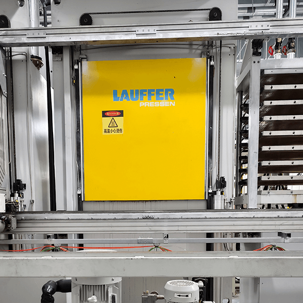
Stack the inner layer board, semi cured sheet, and outer copper foil that have undergone blackening (or browning) treatment according to design requirements, and melt and solidify the semi cured sheet through high temperature and high pressure to tightly bond the layers together, forming a multi-layer board structure. During the compression process, the control of temperature, pressure, and time is crucial, and an appropriate compression curve should be developed based on the material properties.
For example, the compression temperature of FR-4 material is usually between 180-200 ℃, the pressure is between 5-10MPa, and the insulation and pressure holding time is about 60-90 minutes. At the same time, it is necessary to ensure the temperature uniformity and pressure consistency of the compression equipment to prevent defects such as delamination and bubbles.
3、 Key Technologies and Challenges of PCB Inner Layer Process
(1) High precision circuit manufacturing technology
With the development of electronic products towards miniaturization and high density, the requirements for the accuracy of PCB inner layer circuits are becoming increasingly high. At present, the industry has been able to achieve linewidth/spacing of 3mil (about 75 μ m) or even smaller. To meet this demand, more advanced exposure equipment (such as laser direct writing exposure machines), high-precision film production technology, and optimized etching process parameters need to be adopted. In addition, it is necessary to address issues such as signal integrity and impedance control caused by the reduction in line size.

(2) Interlayer alignment technology
The precise alignment between the inner layers of a multi-layer board is the key to ensuring correct electrical connections. During the compression process, interlayer displacement is easily caused by factors such as differences in thermal expansion coefficients of materials and process fluctuations. To improve alignment accuracy, high-precision positioning systems such as pin positioning, optical positioning, etc. are often used, and positioning holes are reasonably arranged in the design stage. At the same time, the compression process parameters are optimized to reduce the influence of thermal and mechanical stresses on interlayer alignment.
(3) Environmental Protection Process Technology
With increasingly strict environmental regulations, the inner layer process of PCB is also facing the challenge of green manufacturing. Traditional etching and blackening solutions contain a large amount of heavy metals and harmful chemicals, which require the use of more environmentally friendly processes and materials as substitutes. For example, using ammonia free etching technology, water-based photoresist, environmentally friendly blackening (browning) solution, etc., to reduce the generation of wastewater and exhaust gas and achieve clean production.
4、 Quality control of PCB inner layer process
To ensure the quality of the inner layer process, it is necessary to establish a comprehensive quality control system. Starting from the inspection of raw material storage, strict performance testing is carried out on copper-clad laminates, photoresist, etching solutions, etc; During the production process, real-time monitoring of key process quality is achieved through online detection equipment such as AOI and X-ray; After each batch of products is completed, sampling testing is carried out, including line continuity testing, impedance testing, interlayer bonding force testing, etc. Once quality issues are identified, promptly analyze the causes and take corrective measures, continuously optimize process parameters, and improve product quality stability.
In summary, the PCB inner layer process is a complex and precise manufacturing process that involves numerous technical links and quality control points. With the continuous development of electronic technology, the requirements for the inner layer process of PCB will also continue to increase. Only by conducting in-depth research on process principles, continuously innovating technological methods, and strengthening quality control can high-performance and highly reliable PCB products be manufactured to meet the growing demands of the modern electronics industry.
The above article provides a comprehensive overview of the PCB inner layer process. If you would like to further understand a specific link or have other related needs, please feel free to contact us.