The PCB CTE is a core parameter for measuring the dimensional stability of PCB boards under temperature changes, which directly affects the reliability and lifespan of electronic devices. With the increasing demand for high-density assembly in the fields of 5G communication, automotive electronics, and aerospace, precise control of CTE has become a key technical challenge in PCB manufacturing. This article will comprehensively analyze the technical connotation and application practice of CTE from the perspectives of its physical properties, impact on reliability, material innovation, and process optimization.
—
Table of Contents
1、 The Physical Characteristics of CTE and the Reliability Challenge of Multilayer PCB
CTE is defined as the linear expansion rate of a material per unit temperature change, measured in ppm/℃ (parts per million/degree Celsius). In PCB, CTE needs to distinguish three directions:
-X-Y axis (plane direction): mainly dominated by the CTE of fiberglass cloth, the typical value of FR-4 material is 13-17 ppm/℃;
-Z-axis (thickness direction): determined by the expansion characteristics of the resin, usually 40-60 ppm/℃, and may increase by 5-6 times beyond the glass transition temperature (Tg).
This anisotropic characteristic has multiple impacts on PCB reliability:
1. Risk of solder joint cracking: When a silicon chip (CTE of about 6 ppm/℃) is soldered to an FR-4 substrate (CTE of 14-17 ppm/℃), temperature cycling can cause thermal stress accumulation, especially in BGA packaging, where solder joints may develop microcracks due to shear forces, ultimately leading to failure.
2. PTH fracture: Z-axis expansion can cause tensile stress on the copper plated hole wall. If the copper layer thickness is insufficient (<1.5 ounces), repeated thermal cycling may cause the hole wall to crack, resulting in signal interruption.
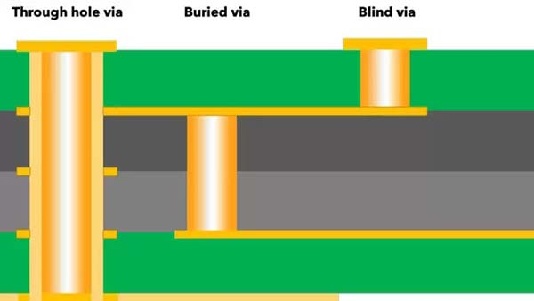
3. Inter layer alignment deviation: The difference in CTE between different layer materials can cause pattern deviation, which needs to be compensated and adjusted through AOL (automatic optical detection) equipment to ensure high-density interconnect accuracy.
—
2、 Innovation and technological breakthroughs in low PCB CTE materials
To address the challenge of CTE mismatch, the industry has achieved breakthroughs through material research and process optimization
1. Selection of high-performance substrates
-Metal core plate: The CTE of copper non expanding steel copper (CIC) and copper molybdenum copper (CMC) are 8 ppm/℃ and 6 ppm/℃, respectively. Combined with the FR-4 outer layer, the overall CTE can be reduced to 9-12 ppm/℃, making it suitable for high-power heat dissipation scenarios.
-Aramid fiber laminated board: The CTE of Kevlar or Aramid materials is 7-8 ppm/℃, and when combined with FR-4, the overall CTE is 12 ppm/℃, significantly reducing thermal stress.
-High Tg resin: Materials with a glass transition temperature exceeding 250 ℃ (such as Shengyi SH260) can maintain Z-axis CTE stability at high temperatures and are suitable for extreme environments in aerospace electronics.
2. Process optimization strategy
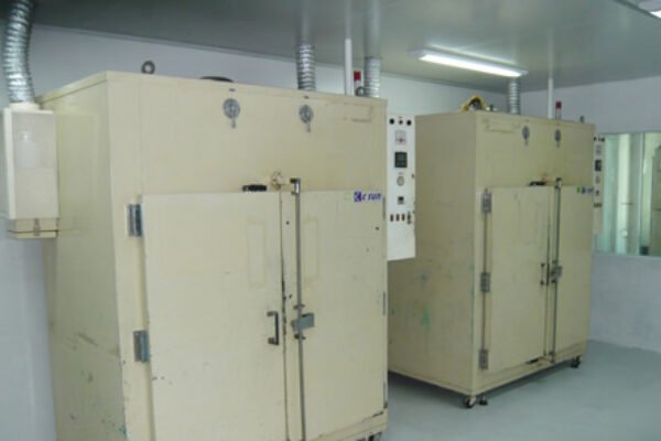
-Laminated control: Adopting a stepped heating and constant pressure curing process to reduce interlayer stress; Dynamic compensation technology can control the laminated offset within ± 25 μ m.

-Copper plating strengthening: Increase the thickness of the through-hole copper layer to over 1.5 ounces, which can withstand more than 3000 thermal cycles and avoid cracking of the hole wall.
-Filler modification: Adding ceramic powder or silicon micro powder to the resin to reduce the Z-axis CTE to below 30 ppm/℃, while improving mechanical strength.
—
3、 CTE matching principle and industry application scenarios
In high reliability fields such as automotive electronics and communication equipment, CTE matching should follow the following principles:
1. Material collaborative design: The CTE of the components should be close to the substrate (such as silicon chips paired with metal core plates), with a difference controlled within ± 5 ppm/℃.
2. Optimization of heat dissipation structure: The thermal conductivity of the metal substrate can reach 2-4 W/m · K, which is 40% higher than traditional FR-4. It can effectively solve the heat dissipation problem when applied to electric vehicle BMS systems.
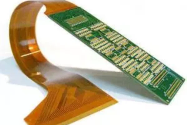
3. Flexible buffer design: In areas with significant differences in CTE (such as chip edges), a rigid flex bonding process is used to release stress through flexible connections.
Typical application cases:
-5G base station: The dielectric loss (Df) of high-frequency microwave boards (such as Rogers RO4350B) is as low as 0.0037, CTE matches with copper foil, and supports signal transmission above 28GHz.
-Medical implant equipment: The flexible PCB thickness of polyimide substrate is only 0.2mm, and the CTE is close to that of human tissue, which can reduce the risk of biocompatibility.
—
4、 Future Trends: Intelligence and Green Manufacturing
1. AI driven process control: By using machine learning to predict defects caused by CTE, combined with AOI optical inspection, the yield rate is increased to 99.95%.

2. Upgrade of environmentally friendly materials: The application of halogen-free substrates and water-based solder mask ink reduces pollution, and the closed-loop etching system achieves a waste liquid recovery rate of over 90%.
3. Nano coating technology: Development of waterproof and corrosion-resistant coatings to expand the application of PCBs in marine exploration and space equipment.
—
Conclusion
CTE control is the core transition of PCB manufacturing from “quantitative change” to “qualitative change”. Through material innovation, process optimization, and intelligent production, enterprises can significantly improve the reliability of their products in extreme environments. Faced with the trend of high-density and miniaturized electronic devices in the future, only by continuously deepening CTE technology can we occupy a competitive high ground in the global industrial chain.