PCB core board, as the core component of printed circuit board (PCB), is a key carrier for electronic products to achieve electrical connection and signal transmission. In a multi-layer PCB structure, the core board is combined with a semi cured sheet through a lamination process to construct a complex circuit network. This article will analyze the core position of chipboards in the modern electronics industry from the perspectives of their definition, manufacturing processes, technological innovation, and future trends.
—
Table of Contents
1、 Definition and core function of PCB core board
PCB core board usually refers to the inner core substrate in multi-layer boards, which is formed by precision processing of copper-clad laminates to form circuit patterns and combined with other layers through lamination technology. As the “skeleton” of electronic devices, the chip board not only supports component assembly, but also undertakes functions such as signal transmission and power distribution. According to different application scenarios, the core board material can be selected from FR-4 epoxy resin, polyimide (flexible substrate), or high-performance special materials (such as Shengyi SH260) to meet the requirements of high temperature resistance and high-frequency signal transmission.

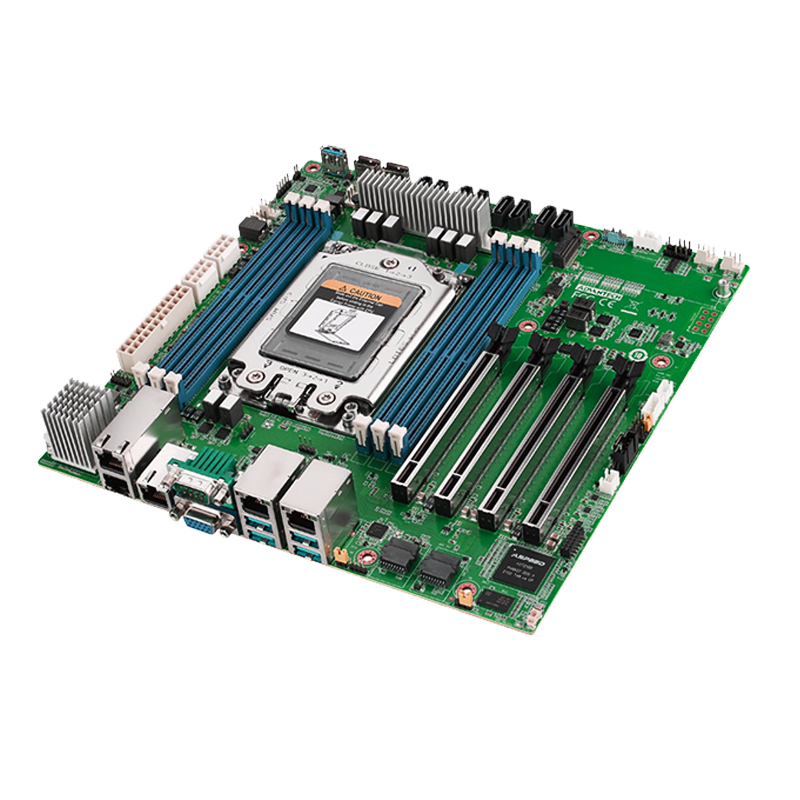
Taking the common 8-layer PCB as an example, its structure is composed of 3 core boards and semi cured sheets alternately stacked, forming high-density interconnects through lamination. The accuracy of the core board directly affects the signal integrity and reliability of the entire board, especially in fields such as 5G communication and aerospace electronics. The performance parameters of the core board (such as dielectric constant and thermal expansion coefficient) need to be strictly matched with the design requirements.
—
2、 PCB Core processes and technological breakthroughs in core board manufacturing
1. Inner layer graphic transfer
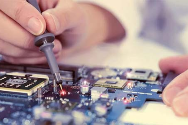
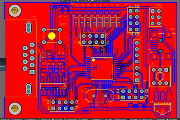
Core board manufacturing begins with the cleaning of copper-clad laminates and the coating of photosensitive films. The circuit pattern is transferred onto copper foil through UV exposure, and the unexposed part is cleaned with alkaline solution and etched to remove excess copper layer, ultimately forming a precision circuit. This process requires a line width control accuracy of ± 10% to ensure low loss transmission of high-frequency signals.
2. Laminated process
Multi layer core boards need to be combined with semi cured sheets through a vacuum hot press machine. Taking the six layer board as an example, after the core board and copper foil are laminated, they are cured for 90 minutes at 180 ℃ and 15kg/cm ² pressure to ensure that there are no bubbles between the layers and the warpage is less than 0.5%. The advanced dynamic compensation system can control the interlayer offset within ± 25 μ m, ensuring the reliability of high-density interconnection.
3. Micro hole processing and metallization
High density interconnect (HDI) core boards require laser drilling technology with a minimum aperture of 50 μ m. The hole wall is formed with a 25 μ m copper layer through chemical copper deposition and electroplating processes to ensure conductivity. The application of pulse electroplating technology improves the uniformity of the coating inside the hole by 15%, avoiding the “dog bone” effect.
—
3、 Cutting edge innovation in chip board technology
1. Research and development of high-performance materials
The aerospace industry has put forward extreme environmental adaptability requirements for core boards. For example, the glass transition temperature (Tg) of Shengyi SH260 sheet exceeds 250 ℃, and its coefficient of thermal expansion (CTE) matches the height of the copper layer, which can withstand temperature fluctuations from -55 ℃ to 250 ℃. It is applied in rocket engine monitoring systems and satellite power modules, significantly improving signal stability.

2. Ultra thin and flexible trends
Smart wearable devices are driving the development of ultra-thin chipboards. The hunting board PCB adopts a combination of polyimide substrate and rigid flex technology to achieve a bendable design with a thickness of 0.2mm. At the same time, it integrates blind buried holes through HDI technology to meet the space limitations of foldable screen phones and micro medical implant devices.
3. Green manufacturing and intelligent production
Environmental protection requirements have spurred the application of halogen-free substrates and water-based solder mask inks. Core material and circuit companies have increased the waste liquid recovery rate to 90% through closed-loop etching systems. The AI defect prediction system combined with AOI optical inspection has increased the yield to 99.95%, accelerating the mass production of high-end chip boards.
—
4、 Application scenarios and future prospects of chip boards
Core board technology has penetrated into multiple core areas:
-Communication equipment: 5G base stations require high-frequency microwave core boards with a dielectric loss (Df) as low as 0.007, supporting signal transmission above 28GHz.
-Automotive Electronics: The Battery Management System (BMS) for electric vehicles uses a metal based core board, which increases thermal conductivity by 40% and solves the problem of heat dissipation.
-Medical equipment: Cardiac pacemakers use biocompatible chips to reduce solder joints and improve long-term reliability through embedded components.
In the future, with the popularization of artificial intelligence and the Internet of Things, chipboards will develop towards higher density and intelligence. Nano coating technology can enhance waterproofing and corrosion resistance, and expand to the fields of ocean exploration and space equipment. At the same time, industrial integration and environmental upgrading will promote the transformation of chip manufacturing towards intensive and sustainable modes.
—
Conclusion
The technological innovation of PCB core boards is a microcosm of the development of the electronics industry. From material breakthroughs to process optimization, chipboards are empowering various industries with higher precision and stronger reliability. As a PCB enterprise, we must continue to deepen our core technology in chip boards, embrace intelligence and green manufacturing, in order to occupy a leading position in the global industrial chain.