Table of Contents
Executive Summary
The journey from Artificial General Intelligence (AGI) to Artificial Superintelligence (ASI) represents the next frontier in artificial intelligence evolution. While algorithms and data capture much attention, the physical hardware foundation—particularly advanced printed circuit boards (PCBs)—will play a decisive role in enabling this transition. This article explores the hardware requirements for ASI development, the specific PCB technologies essential for supporting superintelligence infrastructure, and how the PCB industry is evolving to meet these extraordinary demands. As AI progresses through three distinct evolutionary phases—from current capabilities toward self-iterating superintelligence—each stage presents unique challenges and opportunities for PCB design and manufacturing.
1.Understanding the AI Evolutionary Path: From AGI to ASI
The evolution of artificial intelligence follows a structured pathway toward increasingly capable systems. According to industry leaders like Alibaba’s CEO Wu Yongming, this progression occurs through three distinct phases that represent fundamental shifts in AI capabilities .
Table: The Three Evolutionary Stages of Artificial Intelligence
| Stage | Key Characteristics | Current Status | Hardware Implications |
| Stage 1: Intelligent Emergence | AI learns from human knowledge, develops generalization capabilities | Largely achieved | High-bandwidth training infrastructure |
| Stage 2: Autonomous Action | AI uses tools, codes, interacts with physical world | Current phase | Low-latency, high-reliability PCBs for real-world interaction |
| Stage 3: Self-Iteration | AI improves itself, connects to physical world data streams | Future development | Ultra-high-density, extreme-performance computing infrastructure |
The transition from AGI to ASI represents a quantum leap in capability requirements. While AGI aims to match human-level performance across diverse tasks, ASI envisions systems that surpass human intelligence and possess self-iteration capabilities . This advancement demands unprecedented computational resources that current hardware struggles to provide. Technology leaders including Alibaba are investing heavily—with commitments reaching ¥380 billion in AI infrastructure—recognizing that ASI development requires fundamental improvements in computational density, energy efficiency, and interconnection capabilities .
2.Hardware Foundations for ASI Development
The hardware requirements for advancing from AGI to ASI differ dramatically from conventional computing needs. While current AI infrastructure focuses on training large models, ASI development demands systems capable of continuous self-improvement and real-world interaction.
2.1 The Computational Demands of Self-Iterating Systems
ASI systems require computational resources that dwarf today’s AI infrastructure. Where current AI training might utilize thousands of GPUs, ASI development could necessitate millions of processing units working in concert . This scale presents unprecedented challenges in power delivery, thermal management, and interconnection density.
The shift from CPU-centric to GPU-centric computing in AI data centers is just the beginning. Future ASI infrastructure will require specialized processors optimized for recursive self-improvement algorithms, necessitating custom PCB designs that can support heterogeneous computing architectures with varying voltage requirements, signal integrity needs, and thermal characteristics .
2.2 The Physical AI Interface Challenge
A critical aspect of ASI development involves connecting AI systems directly to physical world data streams. As Wu Yongming notes, current AI excels in domains with human-defined knowledge (like content creation and mathematics) but struggles with raw physical world data . Bridging this gap requires sophisticated sensor networks and interface hardware that can provide ASI systems with comprehensive, real-time environmental data.
This “Physical AI” paradigm—exemplified by collaborations like that between Alibaba and NVIDIA—requires PCBs that can support diverse sensor arrays while maintaining synchronization across data acquisition systems . These applications demand robust designs capable of operating in varied environmental conditions with high reliability.
3.Critical PCB Technologies for ASI Infrastructure
Supporting ASI development requires advances across multiple PCB technology domains. Several specific areas of innovation are particularly crucial for meeting the extreme demands of superintelligence infrastructure.
3.1 High-Layer Count and HDI PCBs
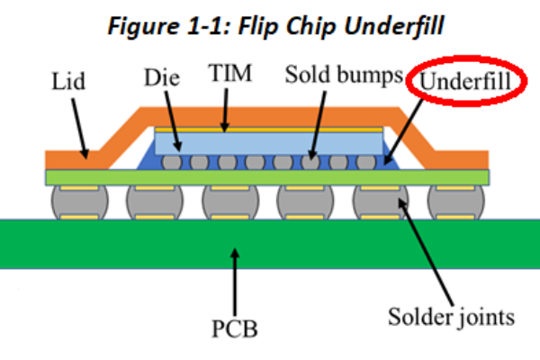
AI servers already utilize high-layer count PCBs (10+ layers) to accommodate complex routing requirements, with advanced designs reaching 24 layers or more . These multilayer boards incorporate blind vias, back drilling, and resin-filled vias to maintain signal integrity at high frequencies . For ASI applications, layer counts will likely increase further, requiring advanced stack-up designs and material selections to manage signal degradation and power distribution challenges.
The industry is moving toward more sophisticated HDI (High-Density Interconnect) technologies, with progression from 2-3 step HDI to 5-6 step HDI designs to support increasingly complex interconnection requirements . This evolution enables higher component density and more efficient routing—critical factors for building the compact, high-performance systems needed for ASI research.
3.2 Advanced Materials for High-Frequency Operation
ASI systems will operate at frequencies far beyond current AI infrastructure, necessitating specialized materials that minimize signal loss. While standard FR-4 materials serve many applications, high-frequency designs require advanced substrates with controlled dielectric properties .
Table: PCB Material Requirements for AI/ASI Applications
| Material Property | Conventional AI | ASI Requirements | Key Challenges |
| Dielectric Constant | 3.5-4.5 | 2.5-3.5 (tight tolerance) | Signal propagation speed |
| Loss Tangent | 0.02-0.03 | <0.001-0.002 | Signal integrity at high frequencies |
| Thermal Conductivity | Standard | Enhanced (≥0.5 W/m/K) | Heat dissipation from high-power components |
| Dimensional Stability | Standard | High stability across temperature ranges | Impedance control |
Materials like M7N high-speed substrates already support higher frequency signal transmission in current AI servers . For ASI systems, materials with even better performance characteristics will be essential, particularly those supporting frequencies above 112Gbps and eventually into the terahertz range for specialized applications.
3.3 Precision Impedance Control and Signal Integrity
Maintaining signal integrity becomes increasingly challenging as data rates escalate. ASI systems will require tighter impedance control than current AI infrastructure, with tolerances potentially needing to move from the current ±10% to ±5% or better for critical signals .
Advanced techniques for impedance management include:
– Precise etch factor compensation to maintain consistent trace geometry
– Controlled dielectric thickness during lamination processes
– Advanced simulation models that account for material variability
– In-line testing methodologies to verify impedance characteristics
These approaches ensure that high-speed signals—particularly those carrying critical synchronization information between processing elements—arrive with minimal distortion, reducing bit error rates in ASI systems .
4.PCB Design Innovations for AI Evolution
Each stage of AI evolution presents distinct PCB design challenges that require specialized approaches and innovations.
4.1 Current Generation AI Server Designs
Today’s AI servers already incorporate advanced PCB technologies to support demanding computational workloads. Modern AI server motherboards are significantly larger than traditional server boards to accommodate additional components, including multiple PCIe slots (5+), expanded memory sockets (4+), and often multiple CPU sockets .
These designs implement sophisticated features such as:
– Back drilling to remove signal stub effects that degrade signal integrity
– High aspect ratio designs enabling higher wiring density
– Dual-sided resin plugging to facilitate higher component density
– N+C+N symmetrical lamination structures to prevent warping in thick, multilayer boards
These technologies support the current phase of AI development, particularly the transition to autonomous action capabilities where AI systems increasingly interact with both digital and physical environments .
4.2 Emerging Requirements for ASI Development
As AI progresses toward self-iteration, PCB designs must evolve to support new architectural paradigms. Key emerging requirements include:
Enhanced Thermal Management: ASI systems will generate unprecedented thermal densities, requiring innovative cooling approaches such as direct liquid cooling, vapor chambers, and embedded thermal pathways within the PCB structure itself. These solutions must manage heat loads potentially exceeding current designs by an order of magnitude.
Power Delivery Networks: The power requirements for ASI systems will necessitate high-current power delivery with minimal voltage drop. This demands thick power planes, strategic via placement, and sophisticated decoupling strategies to maintain stable voltages under rapidly changing computational loads.
Reliability Engineering: As ASI systems take on more critical functions, their hardware must demonstrate exceptional reliability. This requires designs with built-in redundancy, advanced failure prediction capabilities, and robust construction techniques that ensure continuous operation even under demanding conditions.
5.Manufacturing Challenges and Solutions
Producing PCBs capable of meeting ASI requirements presents significant manufacturing challenges that push the boundaries of current capabilities.
5.1 Precision Manufacturing Tolerances
The dimensional tolerances required for ASI-grade PCBs exceed those of conventional designs. Manufacturers must control features such as trace width, spacing, and dielectric thickness with unprecedented precision to maintain consistent electrical characteristics across large board areas .
Advanced process control techniques include:
– Automated Optical Inspection (AOI) systems with enhanced resolution capabilities
– Laser direct imaging for finer feature definition
– Controlled impedance testing on 100% of critical circuits
– Statistical process control methods that minimize variability
These approaches ensure that PCBs meet the strict requirements necessary for reliable operation in ASI systems .
5.2 Thermal Management During Manufacturing
The manufacturing process itself presents thermal challenges, particularly when working with advanced materials that have specific thermal requirements. For example, some high-performance materials require precise control of heating rates during lamination (≥4 K/min) to achieve optimal properties without damaging delicate structures .
Manufacturers have developed specialized approaches to address these challenges, including:
– Custom lamination cycles tailored to specific material combinations
– Advanced press technology that ensures uniform temperature distribution
– Pre-lamination stress relief techniques that minimize warpage in complex, multilayer stacks
These methods enable production of the reliable, high-performance PCBs required for ASI infrastructure .
6.The Future PCB Landscape for ASI Realization
As AI progresses toward superintelligence, the PCB industry must anticipate and prepare for increasingly demanding requirements.
6.1 Technology Roadmaps and Development Timelines
The transition from current AI systems to ASI will occur gradually, with hardware requirements evolving through distinct phases. Industry projections suggest that AI-related PCB demand will grow significantly, with estimates projecting the market to reach ¥69.3 billion by 2026, representing a 64% year-over-year increase .
This growth will drive innovation across multiple PCB technology domains, including:
– Embedded component technology that integrates active devices within the PCB structure
– Advanced packaging substrates that support higher pin counts and faster signal speeds
– Materials science innovations that deliver better electrical and thermal performance
– Additive manufacturing approaches that enable more complex geometries
6.2 Infrastructure Scaling Challenges
Supporting ASI development requires not just advanced PCBs but massive infrastructure scaling. Industry leaders project that data center energy consumption may increase 10-fold by 2032 compared to 2022 levels to support advanced AI capabilities . This scaling presents both challenges and opportunities for PCB manufacturers, who must balance performance requirements with energy efficiency considerations.
The PCB industry’s ability to deliver solutions that support higher computational densities while managing power consumption will be a critical factor in determining the pace of ASI development.
7.Conclusion: Preparing for the ASI Era
The transition from AGI to ASI represents both a monumental technical challenge and a significant opportunity for the PCB industry. As AI systems evolve through phases of intelligent emergence, autonomous action, and eventually self-iteration, their hardware requirements will escalate dramatically. PCBs—as the fundamental interconnection platform—will play a crucial role in determining how quickly and effectively this evolution occurs.
For PCB manufacturers, supporting the ASI revolution requires:
– Continuous innovation in materials, processes, and design methodologies
– Strategic focus on high-performance computing applications
– Collaborative partnerships with AI hardware developers
– Anticipatory research into future requirements beyond current capabilities
The companies that lead in developing PCBs for AI applications today will be best positioned to support the extraordinary demands of tomorrow’s ASI systems. By advancing the state of the art in high-density interconnect technology, signal integrity management, and thermal performance, the PCB industry can help accelerate progress toward artificial superintelligence while ensuring these systems are built on a foundation of reliable, high-performance hardware.
Partner with Us for Next-Generation AI Hardware Solutions
As artificial intelligence progresses toward superintelligence, the demands on underlying hardware will intensify dramatically. Our expertise in advanced PCB manufacturing positions us uniquely to support the development of cutting-edge AI infrastructure. From high-layer count boards for AI servers to specialized substrates for high-frequency applications, we provide the technological foundation for tomorrow’s AI breakthroughs.
Contact us today to discuss how our PCB capabilities can support your AI hardware requirements and help build the infrastructure needed for the next stage of artificial intelligence evolution.